Hardware
Brief overview of the portions of the blimp hardware used in this project.
Lab Components:
+ eZ430-RF2500 Wireless Development Tool
- Uses IAR Embedded Workbench Integrated Development Environment (IDE) or Code Composer Essentials (CCE) to wire/download/debug applications
- Utilizes Spy Bi-Wire and MSP430 Application UART to remotely send/receive data from a PC
- Designed with 21 available development pins and ultra-low-power MSP430 MCU with 16-Mhz performance
- Has two digital I/O pins for LEDs and interruptible push button
- Support for MSP430F20xx and MSP430F22xx families
- Includes a USB-powered emulator for debugging
- Utilizes USB port for power (no external power supply needed) or uses AAA batteries (with Battery Expansion Board use only)
+MSP430-eZ430U Debugging Interface
- Uses IAR Embedded Workbench Integrated Development Environment (IDE) or Code Composer Essentials (CCE) to wire/download/debug applications
- Designed with 14 pins for debugging and one digital I/O pin for LED indicator
- Utilizes USB port for power (no external power supply needed)
- Support for MSP430F200x, MSP430F201x, MSP430G2x01, MSP430G2x11, MSP430G2x21, and MSP430G2x31 families
- Supports some 2xx Spy Bi-Wire devices
- Supports eZ430-RF2500T target boards
Microcontrollers:
+MSP430F2274
- Uses IAR Embedded Workbench Integrated Development Environment (IDE) or Code Composer Essentials (CCE) to wire/download/debug applications
- Designed with 14 pins for debugging and one digital I/O pin for LED indicator
- Utilizes USB port for power (no external power supply needed)
- Support for MSP430F200x, MSP430F201x, MSP430G2x01, MSP430G2x11, MSP430G2x21, and MSP430G2x31 families
- Supports some 2xx Spy Bi-Wire devices
- Supports eZ430-RF2500T target boards
+MSP430F5510
- Low Supply-Voltage Range (1.8 V to 3.6 V)
- Active Mode (AM): 195 µA/MHz at 8 MHz/3V (Typical Flash Program Execution) and 115 µA/MHz at 8 MHz/3V (Typical RAM Program Execution)
- Wake-Up From Standby Less Than 5 µs
- 16-Bit RISC Architecture, Extended Memory, Up to 25-MHz System Clock
- Unified Clock System with FLL Control Loop (for Frequency Stabilization), Low-Power Low-Frequency Internal Clock Source (VLO), Low-Frequency Trimmed Internal Reference Source (REFO), and 32-kHz Watch Crystals (XT1)
- Two Universal Serial Communication Interfaces (USCI_A0 and USCI_A1) with Enhanced UART support
- 10-Bit Analog-to-Digital (A/D) Converter With Window Comparator
- 16-Bit Timer TA0, Timer_A With Five Capture/Compare Registers
- 16-Bit Timer TA1, Timer_A With Three Capture/Compare Registers
- 16-Bit Timer TA2, Timer_A With Three Capture/Compare Registers
Other Equipment:
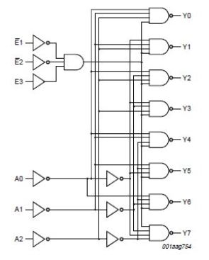
+74HC238 3-to-8 line decoder/demultiplexer
- Demultiplexing capability
- Multiple input enable for easy expansion
- Ideal for memory chip select decoding
- Active HIGH mutually exclusive outputs
- Multiple package options
- Complies with JEDEC standard no. 7A
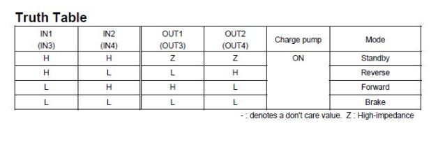
+LV8405 Sanyo Forward/Reverse Motor Driver IC
- 2ch Forward/Reverse Motor Driver
- Low Power Consumption
- Low-temperature Resistance 0.75Ω
- Built-in Low Voltage Reset and Thermal Shutdown Circuit
- Four Mode Function Forward/Reverse, Brake, Stop
+Standard Giant Office Paper Clips
+Aluminum Balloon
+E-flite EFLB5001S Battery
- LiPo 1.9Wh (3.7V) battery
Additional Information: