CSE370 Laboratory Assignment 7
Design Project
Distributed: 25 February 2004
Due: 10 March 2004 (both lab sections)
Objectives
In this laboratory assignment you will decode a hex keypad and transmit the value of the key pressed over RS232 to a computer(see lecture_slides). You are provided with a schematic and two incomplete Verilog description files (KeyPad_Decode and SerialEncoder) that you must complete. Once you have completed the modules and have verified them in simulation, you will then synthesize these two parts into PALs and wire up the entire circuit. You will connect your XLA5 board to a PC running HyperTerminal to provide the characters to display and send them over the RS232 cable. There will be a possibility for extra credit in this project.
Design Files
To create your own design for this project, load the following files into Active-HDL:
Tasks:
NOTE: You can work with your laboratory partner on this assignment but please don't collaborate between groups. You will turn in a single copy of written material with both of your names on it.
- Determine how the keypad works. The keypad has nine pins, four connected to rows, four connected to columns, and one common pin. Plug the keypad into your protoboard and use your logic probe to determine the keypad's wiring.
- Complete the design of the KeyPad_Decode and SerialEncoder Verilog modules. You will need to turn in BOTH the Verilog code and a state diagram for each module.
- Simulate your complete design using the block diagram provided. Turn in simulation waveforms that clearly show a key being pressed causing the corresponding RS232 stream to be generated. Make sure to include all signals of interest in the simulation waveforms.
- Wire up the circuit using the provided
schematic as a guide. Here are details on hooking up the
keypad:
By now, you'll should have completed the design of your two PALs and verified their operation in the simulator. You'll have to decide on your own pin assignments for the PALs, there is a section below that talks about how to create wiring files.
The FPGA has a module called serial_buffer that takes your serial stream and sends it to the computer at 9600 baud. The serial_buffer module is already loaded into the FPGA (see schematic). The FPGA has the following interface:
- O1-- Clock signal output
- O2-- Your RS232 stream from your SerialEncoder
- O3-- DO NOT CONNECT ANYTHING TO IT!
- SW8-- Toggle control for clock.
- "0"-- Single Pulse Mode
- "1"-- Clock continuously running
- LD8-- State of Clock Toggle (see SW8)
- BTN4-- Generate Single Clock Pulse
- LD7-- LED is on when the SerialBuffer is receiving a serial stream on O2.
- LD6/RESET-- Output of the Reset Button (notice this doubles as a LED and as control pin)
- BTN1-- Reset Button
Notice the system already has a reset built in for you so all components will be reset at the same time. Use push-button BTN1 to indicate a reset. The LD6 output of the FPGA makes reset available after it is synchronized and debounced so that you can use it in the rest of your circuit (it is also connected to LD6 for easy viewing).
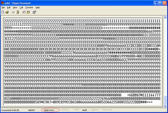
- Use HyperTerminal to view your serial output. Instructions for how to setup HyperTerminal are below. The most important step is to make sure the baud rate is set to 9600 with 8 data-bits, 1 stop-bit, no parity check and no flow control. To connect the serial cable from the PC to the connector on the XLA5 board you will need to add a "null modem" and a "gender changer" between the XLA5 connector and the end of the cable. Make sure to do this. Otherwise, you will not receive characters on to your board. Make sure to keep the null modem and gender changer with your kit, that is, remember to remove them when you unplug your XLA5 board.
- When trying to debug, verify the operation of your circuit a piece at a time. Compare against your simulation waveforms as you single step.
- EXTRA CREDIT: You may notice that many letters are sent while a key is pressed because of the speed at which the system is running. For 20% extra credit modify your project so that when a key is pressed your project will only send the ASCII character once. Basically you need to implement a system to determine when a person releases the pressed key. Keep in mind if a key is misread by your KeyPad_Decoder this will cause nothing to be sent. To complete the extra credit every key press must send its ASCII byte only once. You don't need to worry about the case when multiple keys are pressed. You may use anything in your kit to solve the problem and you may get duplicate parts like PALs from the course staff. Your final solution must fit on your single breadboard. An additional 10% of extra credit will be given for solutions that are done with no additional hardware (wires do not count as hardware).
- Demonstrate your working circuit to a TA on or before March 10. Please hand in your written materials at the March 10 lecture.
Hints:
- When the “received” value of the keypad_decode module is set high, it represents a commitment to the SerialEncoder that keypad_decode will not change the value on its ASCII pins until “receive” is set to low. The only way receive can go low is for the “TXDfinish” to go high letting the keypad_decode module know that it is okay for it to lower “received” and change its value on the ASCII pins. Note that the important part is that the output should not change until received is set to low. This means that the ASCII values should change ONLY when “received” is low.
- The entire circuit is connected to a single Reset button making it possible to bring the entire circuit (including the FPGA) into a known state on the same clock cycle.
- If
you're having trouble making you program fit on the PAL, remember that,
on every clock cycle, a register/output must be evaluated to a 0 or 1
value. If you don't assign a value, the software may have to come up
with a complicated formula to keep values the same.
- We highly recommend that you make an error state so that it is
easy to prevent incorrect values from being transmitted over the
serial. You will loose points if characters that are not present on the
keyboard are transmitted. Common causes of error:
a. Buttons sometimes have bounce giving inconsistent values when they are first pressed
b. Multiple keys being pressed - The output pins in your PAL are not exactly the same; the following table lists the number of possible equations that can be ‘or’ together.
|
Pin |
Number of ‘or’ terms |
|
14 |
8 |
|
15 |
10 |
|
16 |
12 |
|
17 |
14 |
|
18 |
16 |
|
19 |
16 |
|
20 |
14 |
|
21 |
12 |
|
22 |
10 |
|
23 |
8 |
HyperTerminal
The screen shot below shows how to configure HyperTerminal.
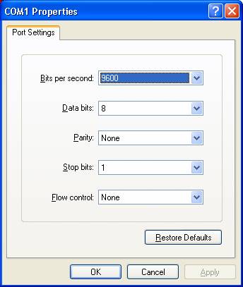
When you run HyperTerm you should see "9600 8-N-1" at the bottom of the window, as shown in the red circle in the figure.
Creating a wiring file for your PAL
To create a wiring file for your PAL you need to create your own CTL file. Refer back to laboratory assignment 6 for an example on proper syntax. Essentially you are creating an attribute by concatenating the various wiring assignments ending the attribute with a semicolon. One important thing to note is that the following 4 items should have the exact same name or your control file might not work.
- The Verilog File (extension .v)
- The Verilog Module
- The Control File (extension .CTL)
- In the attribute declaration line in the CTL file (e.g attribute pin_numbers of [verilog module]:module is)
Review of PAL Programming Method
Place the PAL into the programmer as close to the lever as possible (shown the in figure below where your PAL fits into the red box.)
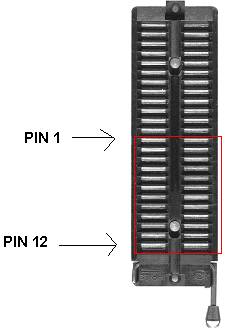
NOTE the location of PIN 1. This means the notch on top of the PAL must be place opposite from the lever.
Programming Steps
- Erase the PAL
- Program the PAL
If ANY of these steps fail try your other PAL. Contact the course staff to help you deal with failures in these steps.
Please be careful with the programmers. Take the time to ensure that you are putting the chip in correctly and that you are following the steps correctly. Refer back to the tutorial for further details.