Lab 7: Useful Components
Overview
Over the last six labs we've learned how to do most kinds of basic logic, but there are still more common elements that are useful for building more and more complex systems. This lab will help you get some experience with them now, and add them to your toolkit in advance of the final project.
Code for this lab
No code provided! Feel free to copy any needed files from previous labs or from lecture as a starting point.
Design Problem – CyberWar
In the last lab, we built a Tug of War game, and by now you've already crushed your roommate into submission. Now it's the hardware's turn. Your goal is to develop a computer opponent to play against, as well as a scorekeeper that can show exactly how badly it beats you…
Counters
We will replace the "winner" system from Lab 6 with counters. Develop a 3-bit counter that satisfies the following behavior:
- Holds a 3-bit state (values 0-7).
- Starts at (and resets to) the value 0.
- When it receives a "win"/"count" input, it increments its current value by 1.
- It doesn't matter what happens when you count past 7 points.
Copy your Lab 6 files and alter them so that there is a counter for each player, each of which drive a 7-segment display with the current score for that player. Whenever someone wins, you increment the appropriate player's score and then restart the game (i.e., reset the playfield). Resetting the entire game will reset the playfield and score, while winning only resets the playfield.
Linear Feedback Shift Registers (LFSRs)
To build a cyber-player, we need to create a random number generator to simulate the button presses of your opponent. In hardware, a simple way to produce pseudo-random numbers is a linear feedback shift register (LFSR). It consists of a set of ℕ D flip-flops (DFF1 to DFFℕ), where the output of DFFi is the input of DFFi+1 (shifting bits linearly). The "randomness" comes from attaching some logical combination of the state bits (feedback) to the input of DFF1. By careful choice of the logical combination, we can get an FSM that is easy to implement but still goes through a fixed pattern of states that appears random.
In this lab, we will use the XNOR of two state bits as our input combination. An example is shown below:
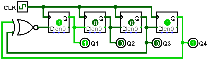
Draw the state diagram for the LFSR shown above. This should show every possible state for the machine (16 total), with transition arrows showing the next state they will enter. Hint: a "*" can be used to label an "always" transition, meaning that regardless of the inputs, we transition to the next state.
Next, create a 9-bit LFSR in Quartus and simulate it. You can find the list of bits to XNOR together by clicking the preview image below. "n" is the number of bits in your shift register (n = 4 for figure 1). "XNOR from" indicates the state bits (numbered starting from 1) to input to your XNOR gate (this is 3 and 4 for figure 1). Following this table will generate the maximum-length LFSR state sequence. How long is the cycle of states for this LFSR (i.e., how many cycles until a state reappears)? Make sure your simulation proves this in whatever way you feel is most appropriate (be creative!). Some example options:
- Split the waveform into multiple screenshots to make things more readable.
- Create an extra signal that only goes high when you're in a particular state.
- Look in the
for how to use printing statements like
$display.
| n | XNOR from | n | XNOR from | n | XNOR from | n | XNOR from |
|---|---|---|---|---|---|---|---|
| 3 | 3,2 | 45 | 45,44,42,41 | 87 | 87,74 | 129 | 129,124 |
| 4 | 4,3 | 46 | 46,45,26,25 | 88 | 88,87,17,16 | 130 | 130,127 |
| 5 | 5,3 | 47 | 47,42 | 89 | 89,51 | 131 | 131,130,84,83 |
| 6 | 6,5 | 48 | 48,47,21,20 | 90 | 90,89,72,71 | 132 | 132,103 |
| 7 | 7,6 | 49 | 49,40 | 91 | 91,90,8,7 | 133 | 133,132,82,81 |
| 8 | 8,6,5,4 | 50 | 50,49,24,23 | 92 | 92,91,80,79 | 134 | 134,77 |
| 9 | 9,5 | 51 | 51,50,36,35 | 93 | 93,91 | 135 | 135,124 |
| 10 | 10,7 | 52 | 52,49 | 94 | 94,73 | 136 | 136,135,11,10 |
| 11 | 11,9 | 53 | 53,52,38,37 | 95 | 95,84 | 137 | 137,116 |
| 12 | 12,6,4,1 | 54 | 54,53,18,17 | 96 | 96,94,49,47 | 138 | 138,137,131,130 |
| 13 | 13,4,3,1 | 55 | 55,31 | 97 | 97,91 | 139 | 139,136,134,131 |
| 14 | 14,5,3,1 | 56 | 56,55,35,34 | 98 | 98,87 | 140 | 140,111 |
| 15 | 15,14 | 57 | 57,50 | 99 | 99,97,54,52 | 141 | 141,140,110,109 |
| 16 | 16,15,13,4 | 58 | 58,39 | 100 | 100,63 | 142 | 142,121 |
| 17 | 17,14 | 59 | 59,58,38,37 | 101 | 101,100,95,94 | 143 | 143,142,123,122 |
| 18 | 18,11 | 60 | 60,59 | 102 | 102,101,36,35 | 144 | 144,143,75,74 |
| 19 | 19,6,2,1 | 61 | 61,60,46,45 | 103 | 103,94 | 145 | 145,93 |
| 20 | 20,17 | 62 | 62,61,6,5 | 104 | 104,103,94,93 | 146 | 146,145,87,86 |
| 21 | 21,19 | 63 | 63,62 | 105 | 105,89 | 147 | 147,146,110,109 |
| 22 | 22,21 | 64 | 64,63,61,60 | 106 | 106,91 | 148 | 148,121 |
| 23 | 23,18 | 65 | 65,47 | 107 | 107,105,44,42 | 149 | 149,148,40,39 |
| 24 | 24,23,22,17 | 66 | 66,65,57,56 | 108 | 108,77 | 150 | 150,97 |
| 25 | 25,22 | 67 | 67,66,58,57 | 109 | 109,108,103,102 | 151 | 151,148 |
| 26 | 26,6,2,1 | 68 | 68,59 | 110 | 110,109,98,97 | 152 | 152,151,87,86 |
| 27 | 27,5,2,1 | 69 | 69,67,42,40 | 111 | 111,101 | 153 | 153,152 |
| 28 | 28,25 | 70 | 70,69,55,54 | 112 | 112,110,69,67 | 154 | 154,152,27,25 |
| 29 | 29,27 | 71 | 71,65 | 113 | 113,104 | 155 | 155,154,124,123 |
| 30 | 30,6,4,1 | 72 | 72,66,25,19 | 114 | 114,113,33,32 | 156 | 156,155,41,40 |
| 31 | 31,28 | 73 | 73,48 | 115 | 115,114,101,100 | 157 | 157,156,131,130 |
| 32 | 32,22,2,1 | 74 | 74,73,59,58 | 116 | 116,115,46,45 | 158 | 158,157,132,131 |
| 33 | 33,20 | 75 | 75,74,65,64 | 117 | 117,115,99,97 | 159 | 159,128 |
| 34 | 34,27,2,1 | 76 | 76,75,41,40 | 118 | 118,85 | 160 | 160,159,142,141 |
| 35 | 35,33 | 77 | 77,76,47,46 | 119 | 119,111 | 161 | 161,143 |
| 36 | 36,25 | 78 | 78,77,59,58 | 120 | 120,113,9,2 | 162 | 162,161,75,74 |
| 37 | 37,5,4,3,2,1 | 79 | 79,70 | 121 | 121,103 | 163 | 163,162,104,103 |
| 38 | 38,6,5,1 | 80 | 80,79,43,42 | 122 | 122,121,63,62 | 164 | 164,163,151,150 |
| 39 | 39,35 | 81 | 81,77 | 123 | 123,121 | 165 | 165,164,135,134 |
| 40 | 40,38,21,19 | 82 | 82,79,47,44 | 124 | 124,87 | 166 | 166,165,128,127 |
| 41 | 41,38 | 83 | 83,82,38,37 | 125 | 125,124,18,17 | 167 | 167,161 |
| 42 | 42,41,20,19 | 84 | 84,71 | 126 | 126,125,90,89 | 168 | 168,166,153,151 |
| 43 | 43,42,38,37 | 85 | 85,84,58,57 | 127 | 127,126 | ||
| 44 | 44,43,18,17 | 86 | 86,85,74,73 | 128 | 128,126,101,99 |
Adders
In class, we developed a circuit for adding binary numbers. Implement either:
- a 9-bit adder with carry out or
- a 10-bit adder
+ or - operators in this module!
Since showing all input combinations for an adder of this size is unreasonable, please simulate enough to cover the situations listed below. If you are unsure what any of these mean, please ask!
- An addition with one input being 0.
- An addition whose result is 511.
- An addition whose result is 0 (other than 0 + 0).
- An example of unsigned overflow.
- An example of positive signed overflow (pos + pos = neg).
- An example of negative signed overflow (neg + neg = pos).
It can be helpful to display signals as decimal or hex values instead of the default binary. To do this, right-click on a multibit signal in ModelSim and select "Radix". Hex and Unsigned are particularly useful choices.
Cyber Player
Now let's implement a tunable cyber player!
- Read through the spec and design requirements carefully.
- Draft a block diagram for your
cyber_warsystem, either from scratch or by modifying your Lab 6 block diagram. - Implement the system according to your block diagram.
- Simulate your overall system to show proper interconnections between modules.
- Finalize your block diagram and submit it with your report.
- Your top-level block diagram should show all of the internal modules and how
they are interconnected.
- Top-level ports should be shown as external inputs and output.
- All instantiated modules should be shown as individual blocks with at least their module name labeled.
- The name and directionality should be clear for all port connections.
- Don't forget an accompanying explanation to help the reader.
Refer to Lab 6's requirements for block diagrams and check any feedback you received on lab reports.
Design Requirements
Slow down the system so you stand a chance by running the game off of divided_clocks[15] (about 768 Hz). If later this still feels too fast or too slow, feel free to use a nearby divided_clock output.
Generate the computer's random button presses using the following procedure:
- Read an unsigned binary value from SW8-SW0 (a value from 0 to 511).
- Using the adder you designed earlier, add the switch value to the LFSR output (another 9-bit unsigned value from 0 to 511).
- If and only if the sum is ≥ 512, the cyber player presses its button. Think carefully about how to determine if the result is ≥ 512 – there is a trivial implementation that will make your life easier!
The switch settings will bias how frequently the cyber player presses its button, making it tunable. Play with the switches to adjust the cyber player's mashing/pulling speed, to see how fast you can go!
Grading
Working Design
100 points for correctness, style, and testing. Include the following files in your Gradescope submission:
- Your
lab6_report.pdf - Your project's SystemVerilog files
- The
.map.rpttiming report file from your project'soutput_filesdirectory
Bonus
Up to 10 points for developing the smallest circuit possible. Follow the same protocal as in Lab 5. Submit your unoptimized SV files to Gradescope first, before attempting to optimize, to ensure you don't lose your working version of the lab. Your final or "active" submission is what we will grade. Note that the "Resource Utilization by Entity" report will give you the sizes of each of the modules in your design, so you can focus your sizing improvement efforts accordingly.