Lab 6: Communicating Sequential Logic
Overview
In the last lab, we developed a single FSM to accomplish our task. Now we want to build a more complex system with multiple, interconnected FSMs. Careful creation of a block diagram, along with design and testing of each individual piece, will be key to getting this working well.
Design Problem – Tug of War
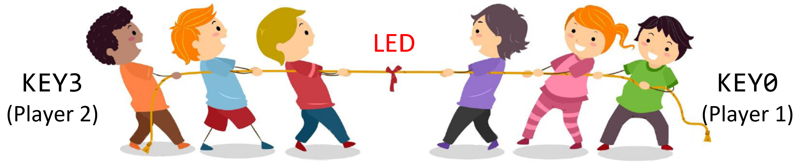
Sweat pouring from their brow, body straining, muscles pulsing back and forth, we have the epic conflict that is Tug Of War! It's time to update this rope-based team sport into an electronic analog of finger-pounding power!
We're going to build a 2-player game using the KEY3 and KEY0 buttons as inputs and LEDR9 to LEDR1 as a 9-light playfield. A single LED on the playfield will be lit to indicate the current position of the "ribbon/knot." A player wins by moving the light off his or her end of the playfield.
Design Rules:
- The "ribbon/knot" starts at the centermost LED (LEDR5).
- Player 1 presses KEY0 to move the light one LED to the right and Player 2 presses KEY3 to move the light one LED to the left.
- When a player wins, display the number (1 or 2) of the victor on the 7-segment display HEX0.
- Use SW9 as the reset signal.
- You should use the 50 MHz clock directly (pin CLOCK_50) to control the whole design – we'll assume no player can press the button faster than 25 million times a second…
If you tried to design the entire game as one big state machine, it would get pretty complex and testing would be incredibly difficult. Instead, we are asking you to break it down into smaller pieces for easier testing and for practice making interconnections between different parts of a system.
Block Diagram
- Read through the whole spec.
- Think about your modules and how they connect.
- Sketch a rough draft of your top level block diagram. Your top level module should be called
tug_of_war. If you've had trouble renaming your top-level module to something other than - After finishing the lab, come back and edit this block diagram to reflect your final design and include it in your report.
DE1-SoC in the past, come see us in office hours to help you out.
Top-level block diagram requirements:
- Top-level ports should be shown as external inputs and output.
- All instantiated modules should be shown as individual blocks with their module name labeled. Port names on the blocks should be labelled if otherwise ambiguous.
- All instantiated modules' ports should be clearly connected.
- The name and directionality should be clear for all port connections.
- All bus widths should be indicated.
- An accompanying explanation to help the reader.
User Input
To deal with metastability, make sure you send each user input
through a chain of two back-to-back flip flops before you use it in your
logic.
This is known as a flip-flop synchronizer. We have provided the module synch (code), for your use.
Create a test bench to ensure it works as expected.
You don't need to worry about metastability too much in this class— as long as you're using the
synch module it will be practically a non-issue. It's just important to remember that we need to use it.
Since our clock is fast, each button press will span many cycles.
We have provided the module pulse (code), for your use.
It works as an edge detector (i.e., its output is high for only 1
cycle for every button press, no matter how long).
Draw a FSM diagram for this module and create a test bench to ensure it works as expected.
user_input, but we
recommend designing them separately for simplicity.
Be aware that these will introduce delays in simulation.
Playfield
It is certainly possible to design a single FSM for all 9 lights; however, we want you to design an FSM for each location (LED). A given playfield light needs to know the following:
- Does it start as True or False?
- Which button(s) were just pressed?
- Am I currently lit? Are my right and left neighbors currently lit?
With this information plus the reset signal, it's now possible to
figure out whether or not this light should be lit during the
next clock cycle.
Suggested SystemVerilog starter code for a light can be found in
normal_light.sv (code).
You may want to create a separate, but similar, module for the center
light, center_light, but depending on your implementation it may be unnecessary.
Victory
You can tell when someone wins by watching the ends of the playfield
– when the leftmost LED is lit and only the left button is
pressed, the left player wins.
Similar logic can be found for the right player.
Build a module, victory that controls the HEX0
display based on these victory conditions.
Suggested Interconnections
The modules you design will read user input from KEYs and control the playfield (LEDR) and victory output lights (HEX). The modules described above are only suggestions. You are free to create the design using any number of different modules as long as it is not a single, monolithic FSM and that you make sure that you can fully reset your system without having to power it off and on again.
Build each of the pieces and test them independently in ModelSim before combining them together. To emphasize: test each element in isolation in modelsim before trying to hook them all up, and test the whole thing in modelsim before downloading to the FPGA!! If you try to do everything by just downloading it to the FPGA you will have lots of trouble getting this lab working, and subsequent labs will be much harder – simulation and good test benches are your friend, and will significantly speed up your debugging.
Only once you have all the pieces, and then the entire system, working in ModelSim should you download the design to the FPGA and test the working game (the fun part!).
Grading
Working Design
100 points for correctness, style, and testing. For each module, you must include a state diagram (if it is an FSM), screenshot of the ModelSim simulation, and thorough testbench bench. Also include a ModelSim simulation for the top-level module. Include the following files in your Gradescope submission:
- Your report PDF
- Your project's SystemVerilog files
- The
tug_of_war.map.rpttiming report file from your project'soutput_filesdirectory
Bonus
Up to 10 points for developing the smallest circuit possible. Follow the same protocal as in Lab 5. Submit a unoptimized version to Gradescope first, before submitting your optimized version. Note that the "Resource Utilization by Entity" report will give you the sizes of each of the modules in your design, so you can focus your sizing improvement efforts accordingly.