Lab 5: Sequential Logic
Overview
Now that we have mastered combinational logic, it is time to figure out sequential circuits. In this lab, you will first play with a pre-made finite state machine (FSM) design before designing your own circuit.
Instructions
Task 1 – Mapping Sequential Logic to the FPGA
To understand the sequential logic design, simulation, and execution process we'll use a state machine that has one input w and one output out. The output is true whenever w has been true for the previous two clock cycles (i.e., it recognizes the input sequence 1,1). The SystemVerilog code for the machine is given in simpleFSM.sv (code).
Simulation
To simulate this logic, we not only have to provide the inputs, but must also specify the clock. For that, we can embed some extra logic in the test bench. The test bench for this FSM is found in simpleFSM.sv (code). Simulate the design with ModelSim, and make sure that it works as you expect.
always_ff block.
Clocks are really important to FSMs, so it is useful to set ther grey gridlines in the Wave pane to line up with the positive edger of the clocks. Click on the "Edit Grid & Timeline Properties…" icon in the lower-left corner of the Wave pane:
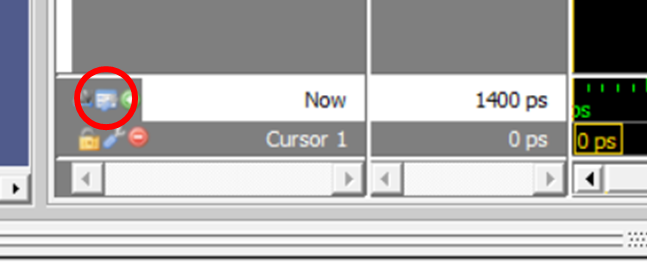
Set the "Grid Period" to 100 ps, which is the simulation clock period (set by parameter CLK_PERIOD = 100;), and the grid lines will line up with the clock. Make sure to save the formatting to the simpleFSM_wave.do file!
Hardware Implementation
To set up the design to run on the FPGA, we need to connect a (real) clock to the circuit, but the clocks on the chip are very fast (50 MHz is a clock cycle every 20 ns). We'd like to use a slower clock, so we provide a clock divider – a circuit that generates slower clocks from a master clock. DE1_SoC.sv (code) is a top-level module that includes a clock divider defined in clock_divider.sv (code) and sets up simpleFSM to use the LEDs and push buttons.
whichClock=25 yields a clock frequency of 0.75 Hz → a clock cycle every 1.33 seconds.
Add the new DE1_SoC.sv and clock_divider.sv to your project, synthesize the design for the FPGA, and test it on the DE1. This design uses KEY0 for reset (i.e., press to reset the circuit) and KEY1 as the w input. LEDR5 shows the clock, LEDR3 shows the reset, and LEDR0 shows the output of the FSM.
You do not have to demonstrate this circuit working, but running this test will help a LOT in getting the design problem working.
Task 2 – Runway Landing Lights
The landing lights at the SeaTac airport are busted, so we have to come up with a new set. In order to show pilots the wind direction across the runways, we will build special wind indicators to put at the ends of all runways at SeaTac.
Your circuit will be given two inputs (SW[1] and SW[0]), which indicate wind direction, and three output LEDs (LEDR[2:0]) to display the corresponding sequence of lights:
P1: 0 1 0

P1: 0 1 0
P2: 1 0 0

P1: 0 1 0
P2: 0 0 1

For each situation, the lights should cycle through the given pattern. In a "Calm" wind, the lights will cycle between the outside lights lit, and the center light lit (two patterns), over and over again. The "Right to Left" and "Left to Right" crosswind indicators repeatedly cycle through three patterns each, which makes the light "move" from right to left or left to right, respectively.
The switches should never both be True. The switches may be changed at any point during the current cycling of the lights, and the lights must switch over to the new pattern as soon as possible. However, it can enter into any point in the other situation's pattern.
- Draw an FSM diagram that uses two input bits and three output bits to implement the runway
landings lights described above. Make sure you include a "reset" transition. Include the diagram in your lab report.
Think carefully about your FSM design! There are multiple ways to do this task, but it's possible to design an FSM that only needs 4 states
Drawing FSM diagrams will generally be your first step when working on sequential circuits. We will expect to see these drawings for all FSMs in future labs. - Once you have your FSM drawn, implement
runway_lightsFSMin SystemVerilog. - Create a test bench
runway_lightsFSM_tbto test your FSM thoroughly. Include an annotated screenshot (or screenshots) of this simulation in your report with a description of how it proves your FSM functions as expected. - Add your FSM to the top-level module
DE1_SoC, replacing thesimpleFSMinstance. Synthesize it and make sure it runs correctly on the DE1 board.
Task 3 – Resource Utilization
After you've synthesized your circuit in Quartus, take a look at the Compilation Report (see figure below). In the left-hand column, select "Analysis & Synthesis" → "Resource Utilization by Entity."
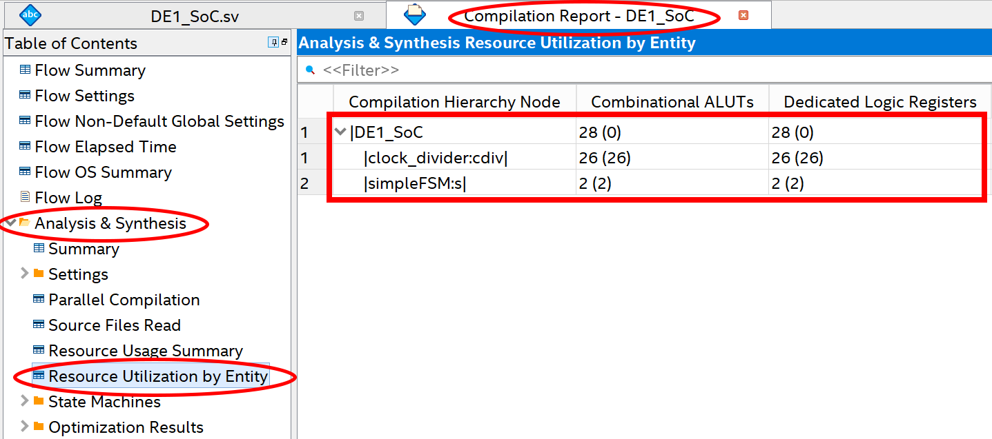
This report breaks down how the various modules in our project take up space on the FPGA. The "Combinational ALUTs" column lists the # of FPGA logic elements being used, and the "Dedicated Logic Registers" is the # of DFFs in use. Each row corresponds to a given module, with the number in parentheses representing the resources just from that module (and not any submodules inside of it), while the number outside of the parentheses is the total resource count (including submodules).
- Include a screenshot of this utilization report in your lab report.
- Calculate your "resource score" by adding the numbers outside the parentheses for the entire design under "Combinational ALUTs" and "Dedicated Logic Registers." and then subtracting the result from that the same numbers from the "clock_divider" line. Include this calculation in your report as wellFor example, the simpleFSM from the first part of this lab has a score of (28+28)-(26+26) = 4, though obviously it doesn't perform the right functions for the runway lights…
- Locate the resource usage report file
output_files/DE1_SoC.map.rptin your project directory. Submit this file alongside your report PDF and your SystemVerilog code. Gradescope will report your resource utilization to a Leaderboard, where students can compare their Resource Utilization for fun. When you submit you can choose the name that appears to the rest of the class next to your resource score; feel free to pick an anonymous name if you like!Note: This is the first quarter we've used the leaderboard feature and we've only tested our autograder on report output from Quartus 17.0.0 (the version available on our course website). In theory it should work for other versions as well, but if it crashsed or doesn't seem to be getting your resource score properly, please let us know in an Ed thread!
Extra credit:
You have the oportunity to earn up to 10 points for developing the
smallest circuit possible, in terms of number of FPGA logic and DFF
resources. If you do choose to pursue this extra credit, please first
complete the assignment normally and submit it on Gradescope.
Then, make a copy of your project folder and report, and work on those. In
your updated report, include both your old resource utilization screenshot
and your new one. State your updated resource score and explain your
optimization design choices. Submit this updated
material on Gradescope when you're done. Your course staff will be
able to see both versions of your work.
Extra credit is determined based on raw numbers rather than the
leaderboard; the Leaderboard just allows you to see how your resource
utilization compares to your peers.
Grading
Working Design
60 points for correctness, style, and testing. Include the following files in your Gradescope submission:
- Your report PDF
- Your project's SystemVerilog files
- The
DE1_SoC.map.rpttiming report file from your project'soutput_filesdirectory
Bonus
Up 10 points for developing the smallest circuit possible, in terms of number of FPGA logic and DFF resources.
Lab demo
40 points for a clear and professional walk-through of your submitted lab material.