A schematic is a drawing that represents all or part of an electronic circuit. For creating schematics Synario provides us with an easy-to-use and powerful Windows-based program. A single schematic may be sufficient to show the entire circuit in terms of it's primitive elements. But a schematic created in the schematic editor can also consist of more than one sheet. The original schematic can be extended by adding as many sheets as desired using appropiate commands from the editor.
Schematic representation of a circuit help in the better understanding and debugging of the circuit. We don't have to worry about the syntax of the language as is the case when we represent our circuit in a hardware description language like ABEL. Schematic basically consists of symbols interconnected with wires which are more easier to understand than an ABEL source code.
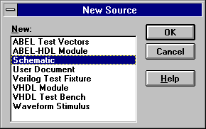
Once we have created a new project using the Project Navigator it is time to create source files for our design. Here, we will see how to create a new schematic and enter symbols into this schematic. We will create a new source file by selecting the "New ..." entry in the "Source" menu. This will provide us with a choice of the type of specification we want to enter. We will then choose "Schematic" as shown below.
We can use the same root name for the schematic as for the project. However, this is not required as there may be multiple schematic drawings for one project.
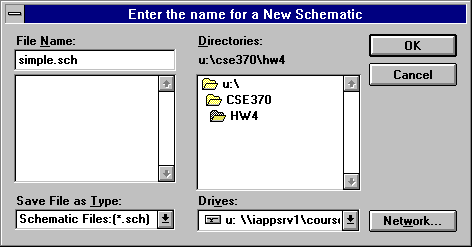
Once we enter the name of the schematic and click on "OK", a schematic diagram editor window will pop-up on the screen. This is the first of the tools of the Synario tool suite that we will be using.
always, and, assign, attribute, begin, buf, bufif0, bufif1 case, casex, casez, cmos, deassign, default, defparam, disable, edge, else, end, endattribute, endcase, endfunction, endmodule, endprimitive, endspecify, endtable, endtask, event, for, force, forever, fork, function, highz0, highz1, if, ifnone, initial, inout, input, integer, join, large, macromodule, medium, module, nand, negedge, nmos, nor, not, notif0, notif1, or, output, parameter, pmos, posedge, primitive, pull0, pull1, pulldown, pullup, rcmos, real, realtime, reg, release, repeat, rnmos, rpmos, rtran, rtranif0, rtranif1, scalared, signed, small, specify, specparam, strength, strong0, strong1, supply0, supply1, table, task, time, tran, tranif0, tranif1, tri, tri0, tri1, triand, trior, trireg, unsigned, vectored, wait, wand, weak0, weak1, while, wire, wor, xnor, xor.
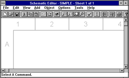
In this tutorial we will build a design that consists of a simple AND gate. To do this, we will
The Schematic Editor allows us to draw gate level schematics by selecting gates and placing them on the document and then connecting them. To draw an AND gate on the drawing, select the "Symbol ..." submenu of the "Add" menu of the Schematic Editor and the following palette for the symbol library should appear.
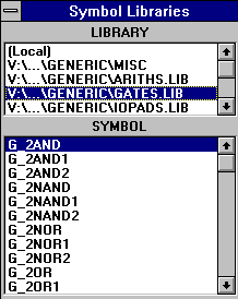
The symbol library is provided by Synario to facilitate starting a schematic diagram. Later on we'll see how to define our own symbols so that our schematics can include hierarchy (elements composed of simpler elements). Select the "GENERIC\GATES.LIB" sub-library. We'll notice that many primitive gates are provided including: AND, OR, NAND, NOR, and NOT. There are versions of the gates with different numbers of inputs (up to 4) and with some of the inputs inverted (bubbles on the inputs). For example, G_2AND is a 2-input AND gate while G_3NAND2 is a 3-input NAND gate with 2 inverted inputs. Select a G_2AND gate and place it in the schematic drawing. Notice that the cursor turns into the gate when we place it over the Schematic Editor window.
The schematic drawing should now look like this:
![]()
Experiment with moving/dragging the symbol around on the drawing by using the items in the "Edit" menu. Try deleting and re-placing another instance of it (by re-selecting it from the library as above). Try zooming in and out on the drawing by using the items in the "View" menu. Lets add some wires to the drawing by using the "Wire" command in the "Add" menu. Wires will be used to connect the inputs and outputs of our AND gate to other elements of our schematic. For now, just add a short wire to each input and output.
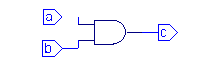
The next step is to add some names to these wires and thus to the inputs and outputs of our AND gate. The name that we give replaces any name the Schematic Editor may already have assigned. We can name the inputs and outputs by using the "Net Name" command of the "Add" menu. Note that the schematic editor prompts for a name at the bottom of its window. Enter a name, say "a", and hit return. The cursor will turn into an "a" and we can click on the end of the wire to which we want to end the name. Notice how the name is automatically adjusted to line up with the end of the wire. Repeat this for the other input and the output of the AND gate so that the schematic now looks like this:
![]()
One important thing to remember is, when two separate nets with the same name are connected, even though no connection appears on the schematic. This feature makes it easy to connect widely spaced components without having to draw long wires across the schematic.
The last step in making our schematic drawing is to add I/O markers that indicate which signals we expect to be the primary inputs and outputs of our entire design. If we don't add these I/O markers we will have trouble verifying the design because Synario wouldn't know what the inputs and outputs to our design are. Hence , this step should not be overlooked. In our case, we'll be interested in naming all three inputs and outputs. However, in larger designs, there may be many internal signals that won't be observable at the pins of the devices we'll use to realize our design. To add I/O markers select "I/O Marker" in the "Add" menu. Select "input" for the type and click on the ends of the inputs wires "a" and "b". Notice that a small arrow shaped box is placed at the end of the wire (pointing in to indicate input). Now do the same for our output to obtain a schematic like the following:
After creating the design specification, the next step is to verify the design. Therefore, save and close the schematic editor window. The project navigator window will now show that a schematic drawing has been entered for this project and it is called "simple" and is stored in the file "simple.sch" which appears in parentheses.
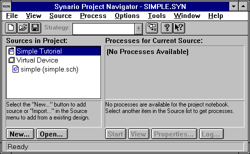
When we select the schematic drawing in the "Sources in Project" sub-window of the project navigator window, we'll notice that a set of things will appear on the right sub-window labeled "Processes for Current Source". These are all the things that Synario can think of to do with our schematic drawing. We may want to navigate its hierarchy, compile it into logic equations, minimize that logic, and/or look at the reduced equations derived from this process. The nice thing about Synario is that it worries about the dependencies between these tools and which files are the inputs to one and the outputs of another. We can simply select the thing we are interested in doing and Synario does it. For example, if we want to see the reduced equations, we can just double-click on that entry in the "Processes" sub-window and whole bunch of activities are started off.
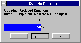
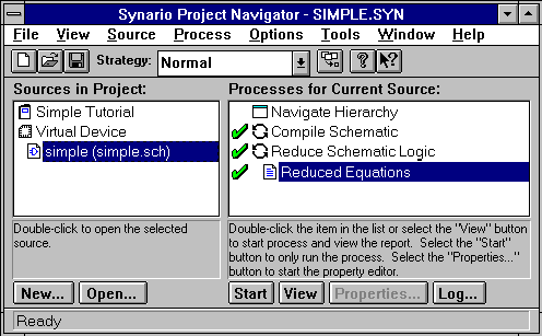
The check marks mean that the process completed successfully. If it had not, we would see either a yellow exclamation point indicating that warnings have been generated or a red "x" indicating that a fatal error had occurred and that the processes could not continue. We can view the results of the operations, that is, the reduced equations, by clicking on the "View" button at the bottom of the "Processes" sub-window. Errors and warnings can be viewed by using the "Log..." button. In this case, the reduced equations file looks like this:
Synario 2.30
Design and created Fri Jan 10 17:24:42 1996
Title: simple.bls
P-Terms Fan-in Fan-out Type Name (attributes)
1/2 2 1 Pin c
====================================
1/2
Best P-Term Total: 1
Total Pins: 3
Total Nodes: 0
Average P-Term/Output: 1
Equations: c = (b & a);
Reverse-Polarity Equations: !c = (!b # !a);
Note that it includes a list of the gates, their fan-in and fan-out values, and the equations for each gate (remember that these can be much more complex than the simple AND gate we are using) as well as the complement function indicated by the Reverse-Polarity Equations.