CSE370 Assignment 5
Distributed: 4 February 2010
Due: 10 February 2010
Reading:
- Katz/Borriello, Contemporary
Logic Design 2e, Chapter 5, Sections 5.1 to 5.4 (pp. 221-234)
- Katz/Borriello, Contemporary
Logic Design 2e, Chapter 6 (pp. 259-299)
Exercises:
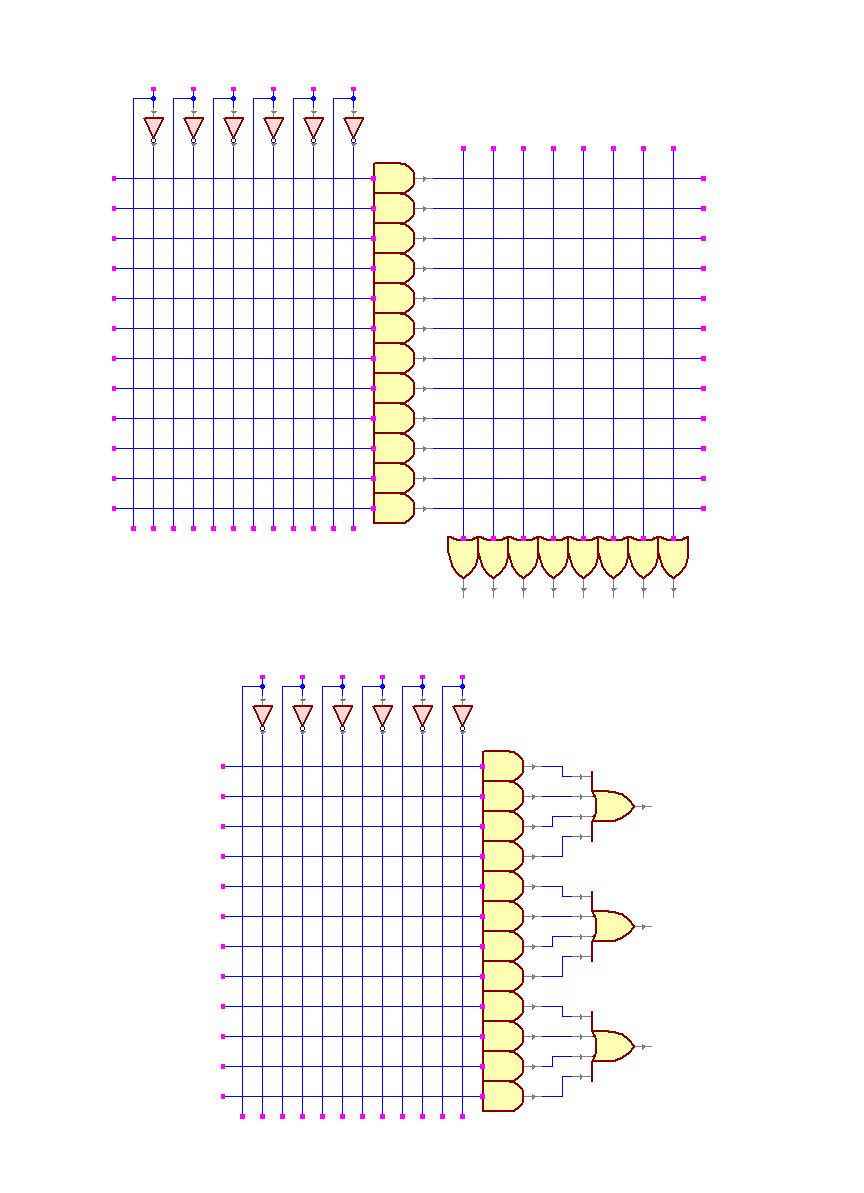
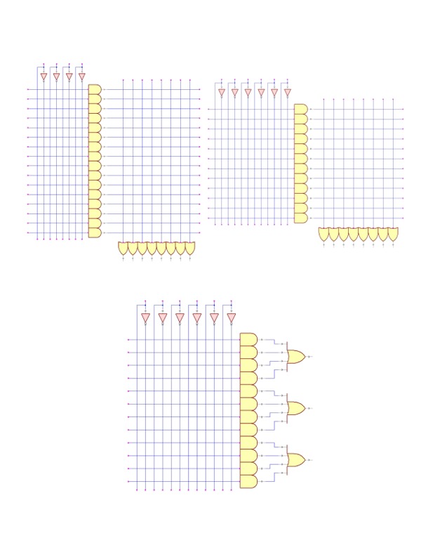
- For the following problems,
you may print the ROM,
PLA
and PAL worksheets or the
worksheet that has all three on one page. Implement the following
three functions using a ROM, PLA and PAL. For the PLA, try to minimize the
number of AND gates you use (fewest terms overall for the 3 functions).
g1(a,b,c,d) = ∑ m(1, 7, 9, 12, 13, 14) + d(3, 11)
g2(a,b,c,d) = ∑ m(7, 9, 15) + d(14)
g3(a,b,c,d) = ∑ m(1, 3, 9, 12, 14) + d(7)
- CLD-II, Chapter 5, problem
5.4
This problem is based on the first exercise in HW#4. You will now come up with a
corresponding combinational logic implementation of your Verilog
description. For part c, only
consider the logic of part b, not the ROM of part a. For this exercise,
you can assume that all the inputs will be correct and you do NOT need to
implement the ERROR output that was in the previous assignment.
- CLD-II, Chapter 6, problem
6.12
- CLD-II, Chapter 6, problem
6.19
Rationale:
- To use two-level regular
logic to implement combinational logic functions.
- To start working with
sequential logic elements.
Comments to: cse370-webmaster@cs.washington.edu