CSE 370 Laboratory
Assignment
Applying Your
Knowledge
Assigned: Monday,
May 24, 2010
Due: End of Lab Section, Wednesday, June 2, 2010 **Note: It is almost the end of
quarter, so it is important you finish this lab quickly to begin work on Lab
9.**
Click
Here for a printable .pdf of this lab
Objectives
You
have gained many invaluable skills over the course of the quarter; you should
now have a good understanding of combinatorial logic, sequential logic,
registers, state diagrams, and other related skills. The final two labs of this
course, lab 8 and 9, will require you to combine all of your skills to develop
a complete system on the FPGA. You will be provided with an output device, an
LCD screen, and an input device, a magnetic stripe card reader, your task is to
get the LCD to display the data stored on magnetic cards swiped through the
magnetic card reader. This is a non-trivial task but one that should amply
demonstrate what you’ve learned this quarter.
Since this task is relatively complex it has been broken into two halves for
you and a lab partner to work on over the course of two lab sessions and time
outside of class. The first half of the lab involves programming the logic that
drives the LCD; like many devices the LCD must be initialized properly, and it
has a specific set of instructions it understands. For now, we will use the
switches on the board to generate the instructions (commands and data) to be
written to the LCD instead of reading data from the magnetic stripe reader.
This will allow you to test to see if your LCD behaves as expected.
Before You Begin
The
first thing you should before beginning this lab is finding yourself a partner.
At your disposal is also the very important datasheet for the LCD: LCD.pdf. This datasheet contains all of the information that
is presented below in the lab, though in much greater detail. It is essential
that you refer to the datasheet for questions about the LCD. You should take
this opportunity in this lab to get some practice reading datasheets and
interpreting the data they can provide.
Tasks:
This
lab write-up will guide you through each component that you will need to create
a working final product. It is strongly recommended that you follow the tips
and guidelines presented in the lab write-up. However, if you are feeling
confident, you are completely welcome to read the datasheet and design the
entire lab independently of the write-up. Just make sure you complete all of
the check off tasks at the bottom of the lab.
The
Clock:
- Now that we have gained some knowledge of sequential
logic we know how important the clock is for the entire system. So why not
just use the clock provided by the FPGA? Take a look at the datasheet: LCD.pdf, under the section labeled as "Timing
Characteristics" what do you see? The most important time is the
Enable Pulse Width which is a minimum width of 450ns (nanoseconds),
however the FPGA’s clock runs at 24Mhz. How fast is that? With that
in mind, you should think about creating a new clock signal that has a
clock cycle that is longer than the 450ns threshold so you can think about
signals changing no closer that one period and therefore don't have to
worry about the setup/hold requirements at a fine-grain. Also note that
some of these LCDs are old and require more than 450 nanoseconds to work
properly and you don't need a very fast clock (your eyes are nowhere near
fast enough to see anything at less than 1ms), so throw in some extra
padding.
How do we solve this problem of creating a new clock? The most logical way is to slow down the clock since we have no control over the internals of the LCD. Look at the provided clock_divider.v file, this Verilog file divides down the original FPGA clock to a slower clock. Make sure you understand how it works because it is incomplete. Set the parameter by filling in a value such that it slows down the clock enough for the LCD to run properly. Have your TA check you off to confirm that you have an acceptable clock speed.
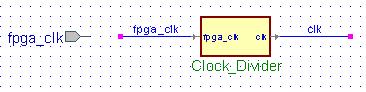
- Now you should create a new design with design flow in
Active-HDL. Add a new file called Lab_8.bde. Create an input called:
fpga_clk and wire up your Clock Divider on the block diagram design. It
should look like the image below when you are finished. Later on when we
write up the .qsf file for the pin assignments we will assign the clock
provided by the FPGA to the fpga_clk input and use the clk output that the
Clock Divider provides as our actual clock.
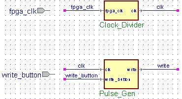
The
Write Button:
- For this lab you will need to control when characters
are written to the LCD by using a button, but in order to write only a
single character at a time it is helpful to bring back the Pulse_Gen
module from the previous lab. This time we provide it: Pulse_Gen.v. Save it to your src/source folder and
wire it up in your bde/block diagram design. Don’t forget to add an
input in your design which represents the button. We will have to remember
to assign a button to this input when we write the .qsf file later on. For
simplicity, use the name: write_button for the name of the input. When you
have wired it up correctly it should look like the image below.
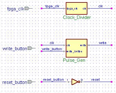
The
Reset Button:
- We need to be able to reset the LCD to clear the screen
whenever we want. The best way to do this is to create a button input that
acts as a reset button. Create an input called: reset_button and wire it
to an inverter with an output called reset. The inverter is used because
the buttons are actually active low. When you press the button, it sets
the wire to a 0, and a 1 when it is not pressed. Once you have wired it up, your
diagram should look like the picture below. Well done, you’ve
finished all the easy stuff!
The
LCD:
- Now that we have finished the easy stuff it’s
time to actually create the logic that will drive the LCD and get it to do
what we want it to do. This information is all contained within the
datasheet: LCD.pdf. The LCD is capable of many
commands; however you will only have to implement a few commands: for
Resetting and Clearing the LCD and writing a character for the LCD to show
on its screen. To aid you, the pins and what they do are displayed below.
The pins are numbered from right to left, when you hold the LCD so that
the pins are closest to you.
|
Pin |
Name |
Function |
||
|
1 |
GND |
Ground - wire GND to it |
||
|
2 |
VDD |
5V - Powers the LCD, wire the 5V red VDD to it |
||
|
3 |
Vo |
1V - Contrast, The LCD needs exactly 1V on this pin so
characters are visible |
||
|
4 |
RS |
High: When RS is high the LCD expects data to come over
the data pins |
||
|
5 |
R/W |
High: When R/W is high the LCD can be read from |
||
|
6 |
E |
This is the Enable, it executes command/data is passed to
the LCD on the negative edge of E |
||
|
7 |
DB0 |
Data Bus 0, this is one bit of data |
||
|
8 |
DB1 |
Data Bus 1, this is one bit of data |
||
|
9 |
DB2 |
Data Bus 2, this is one bit of data |
||
|
10 |
DB3 |
Data Bus 3, this is one bit of data |
||
|
11 |
DB4 |
Data Bus 4, this is one bit of data |
||
|
12 |
DB5 |
Data Bus 5, this is one bit of data |
||
|
13 |
DB6 |
Data Bus 6, this is one bit of data |
||
|
14 |
DB7 |
Data Bus 7, this data bit also acts as an output for the
LCD. When R/W is high and RS is low, the LCD will output a high signal if the
LCD is busy and low signal if the LCD is not busy. |
||
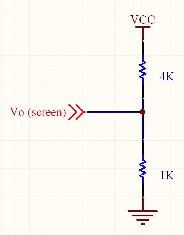
- Make sure you understand each one of these pins and
exactly what they do. You will have to provide a signal for all 14 of
these pins. The first 3 are easy because they are only Ground, VDD, and
Vo. To generate a 1V signal for Vo you will be provided with a 3.9K and 1K
resistor. You can use these two resistors to divide the voltage down to
provide 1V to pin 3 of the LCD. If you don’t understand exactly how
to do this, refer to the picture below. You can visit this site: Resistor Color Codings to
help you identify which resistor is which. Go ahead and wire up the first
3 pins on your board now. Since the FPGA can arbitrarily assign inputs and
outputs to any of the I/O inputs at the bottom of your board you
don’t have to worry about putting your LCD near any particular pins.
LCD
Control Logic:
- Now that we have set up power, ground, and contrast for
the LCD we need to begin to work on the logic that drives the LCD. There
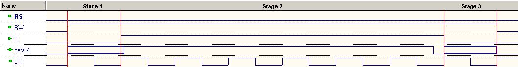
are four key signals that you should keep in mind, RS, R/W, E, and Busy.
From above you know that RS is driven on Pin 4, R/W is driven on Pin 5, E
is driven on Pin 6, and Busy is driven on Pin 14. The goal of the control
logic is to pass the correct signal for RS, R/W, and E based on the Busy
signal. The idea here is: you can’t write to the LCD if it’s
busy, and you can’t pass commands to it either while it’s
busy. Note that according to the timing diagrams on the datasheet, RS and
RW must remain fixed for a cycle (at least long enough to meet setup
times) before E goes high, while E is high, and a cycle after E goes low
(to meet hold times), so keep that in mind when you’re considering
your logic. Take a moment to consider what combinations of signals will be
necessary to execute the following signals: Clear Display (Command),
Function Set (Command), Display On (Command), Entry Mode Set (Command),
Write Character (Data). Make sure you account for the kind of signal and
set RS appropriately. Take a look at the waveform below, familiarize
yourself with the timings of the LCD control logic.
Checking Busy Signal
Waveform:
|
|
|||
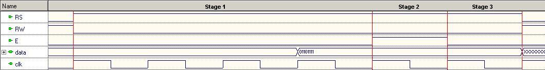
|
Command/Character Write
Waveform:
|
|
|||
|
LCD
Setup Commands:
- The commands: Clear Display, Display On, Entry Mode
Set, and Function Set are the initialization commands that must be passed
to the LCD to prepare the LCD to write characters. Since these are the
initialization commands, they must be executed every single time the LCD
is reset. You should refer to the table below for the execution order, RS
signal, and command encoding for each of these commands.
|
Order |
Operation |
RS |
DB[7:0] |
|
1 |
Clear
Display |
0 |
0000
0001 |
|
2 |
Function
Set |
0 |
0011
0011 |
|
3 |
Display
On |
0 |
0000
1100 |
|
4 |
Entry
Mode Set |
0 |
0000
0110 |
|
5+ |
Write
Character |
1 |
????
???? |
- Before you write any character or command to the LCD
you should check the busy signal first. In fact your first state machine
should always be alternating between checking the busy signal and writing
something to the LCD. You should also think about making a state machine
to keep track of what command you are on or whether you've finished
sending the commands and are now sending characters. Note that for every
command/character the second state machine goes through, the first state machine
must complete a full cycle. This means that the first state machine must
have an output that is used as an input to the second state machine. Also
note that because there is not a steady stream of characters to write
there will be times when you will have to wait in stage 1 of the write
waveform. Whether or not to pause is something the second state machine
must tell the first. There is also the question of how to deal with RS
because its value depends on the state of both machines. Based on the information
that you have now, you should be able to design two simple state
machines/state diagrams that carry out all of the logic described above.
Show your TA your completed state diagrams before moving on.
Programming
States in Verilog:
- Now that your state diagrams are complete it is time to
convert them into Verilog. Your code should be similar in structure to
your controller state machine from Lab 7.
Tri-State
Command and Data:
- By now you must have realized that the 8-Pin DataBus is
shared by two different sets of signals. One is the command signals to
initialize the LCD and the other is the data signals that specify which
character to write to the LCD. We need to tri-state these two sets of
signals so that they don’t interfere with one another. You can do
this in Verilog by specifying the output z, z stands for disconnected or
high-impedance, which basically means the output is electrically
disconnected from the rest of the circuit. You can refer to this article
for some more information on Tri-State Logic .
You will need to do this when writing the Verilog for your LCD logic. An
example is provided for you below on how to tri-state your command signals
and data signals.
|
|
- As you can see from the code above, the OutputEnable
input acts just like a multiplexer control, choosing from the Data
provided as input or the high-impedance z signal. A good example of
tri-state is the LCD that you are working with. Since the LCD can both
output a busy signal and take in a command/character you know it is
tri-stating between those two possibilities. Since the LCD is expecting
either input or output you need to write your code so that it can handle
this case. Sometimes you will be taking an input from the LCD checking for
a busy signal. Other times you will be passing either a command or
character to the LCD. Since you switch between output and input, you're
going to have to tri-state. HINT: In the case of this project, your
tri-state is probably based off RW because it controls whether you are
reading or writing.
In-Out
Buses/Wires
- If you have been paying attention you will notice that
in your block diagram design you need to make your DataBus an output too
because the busy signal comes over on DataBus[7]. If you check under the
icon that usually has inputs and outputs, however there is another option
to make your input/output an in-out instead. This will allow your code to
work when you program it. Just in case you aren’t sure, check the
picture below to make sure it looks right.
![]()
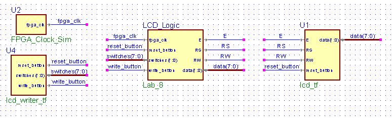
Testing
Your Logic:
- Now that you have worked out your logic your LCD logic
should consist of 4 inputs and 4 outputs. The four inputs should consist
of the clock, reset, write, and an 8-bit switch input. Your four outputs
should consist of E, RS, R/W, and an 8-bit data output. Wire up the
following three pieces in a new test.bde around your LCD logic as shown in
the picture below. You will need these three pieces:
fpga_clock_sim.v
lcd_writer_tf.v
lcd_tf.v
Make sure that the expected message prints out: "Hooray!".
Synthesize
and Demonstrate:
- Now that everything has been tested and seems to work
in simulation you are ready to go ahead and synthesize it and wire it up
on your prototyping board. Use SW0-7 to drive your Switch inputs, use the
24MHz clock to drive your clock input that is divided down. Drive your
write with KEY1 and drive your reset with KEY0. You should run your
outputs to the output pins which you used in the earlier labs. When
writing your .qsf file for this lab, you will have to make connections
from the LCD pins to the IO pins on your prototyping board. The name of
the pins are written on the label on the side of the IO pins. These are
like "A13, B13, etc." You can refer to this page: IO Pins, if you are confused. Make sure everything
is working and demonstrate your working LCD to your TA.
Lab
Demonstration/Turn-In Requirements
A TA
needs to "Check You Off" for each of the tasks listed below.
- Have a TA check you off for your Clock Divider.
- Have a TA check you off for your LCD Logic State
Diagram(s).
- Have a TA check off your working LCD.
Comments
to: cse370-webmaster@cs.washington.edu