CSE370 Laboratory Assignment 7
Counters and Finite
State
Distributed: November 14, 2006
Due: End of Lab Session
Objectives
In this laboratory assignment we will construct two finite state machines. We'll start by making our own '163 counter and then build a simple game FSM. In both cases, we'll only use our 22V10 PAL (see map). This lab will focus on the sequential logic capabilities of the PAL.
Tasks
Part 1
- We'll start by building a
4-bit, loadable and resetable binary counter
with count enable. In fact, it will be a component very similar to a
'163 counter, whose pins and internal logic diagram are reproduced
below. In the datasheet you
will be able to find much more information. Page 5 has a waveform
that shows the basic operation of the counter. If the LOAD signal is
asserted, the A, B, C and D values will be loaded into the output on the
falling clock edge. Similarly, if CLR is asserted (low), it will set
the outputs to 0 on the clock edge. Finally, in normal operation,
the counter will count up sequentially and loop back to 0 after
15. Note that the RCO pin (ripple-carry output) is an output which
goes high when the counter outputs 15. ENP and ENT are enable
pins. The datasheet has a great explanation on page 1 for why the
chip has two enable pins. We've prepared a skeleton
Verilog file for the counter that you must
complete. Note that it uses uncomplemented inputs (active high) for the load and
reset signals. You do not need to
change this to match the actual ‘163 chip. You will also
need a pin assignment file to direct the
tools to assign signals to specific pins of your PAL (you do not need to
change this file, but if you do, keep the same structure).
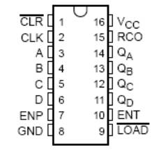
Pin diagram for '163 counter with synchronous reset
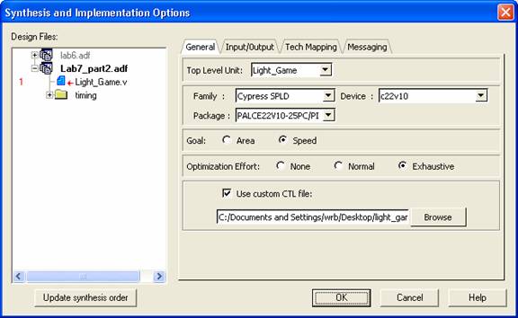
To set the tool to use the pin assignment file (.CTL extension), in the
Synthesis Options window. On the General tab click the check box "Use
Custom CTL file." Next Click on the Browse button and point the program at
your CTL file. Click OK.
After you've compiled your circuit, look at the synthesis report and study the
equations for the flip-flop inputs. Are they what you expected?
Convince yourself that they match the logic diagram below for the '163 (that
they are logically equivalent). Do they differ in any substantial way?
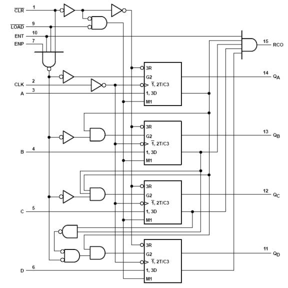
Internal logic diagram for the '163 (the G2 input of the flip-flops is an
enable signal, the 3R input is the synchronous reset signal, and the M1 input
is the load signal).
- Connect your 4 inputs, load,
enable, and clear lines to switches and 4 outputs to LEDs.
Run your counter using the push-button and verify that it is counting
properly. Make sure to use the enable, load, and clear inputs at various
times and check that all work as expected. Show your work to the TA to be
checked off.
Part 2
- We will be constructing a
simple game based on an FSM that we will build using our 22v10 PAL.
The game uses 7 LEDs and two push button
switches. It functions as a simple tug-of-war variant. The game
starts with the middle LED turned on. When one button is pressed,
the light shifts one to the left, when the other button is pressed, the
light shifts one to the right. The objective is to push the button
on one side fast enough to turn on the LED on an end of the line.
When one of these LEDs turns on, one player is
the winner and the game must be reset.
Below is a state diagram for the game FSM. In addition to the main functionality of this state diagram, we also need to ensure that the push buttons only generate a single width pulse for this FSM. To be extra sure, we'll use a flip-flop to create a single pulse whenever the push button input changes from 0 to 1.

State diagram for the game FSM.
We are providing you with a Verilog
file that implements the sequential logic for this game and the pin assignment file to go with it. Compile this
into your PAL. When putting the PAL on your breadboard, use two slider switches
for the left and right inputs and use the push button to generate a clock
signal. Verify that the game works as advertised. Remember to reset
the FSM to start each game.
Two more push buttons have been programmed to work exactly the same as your
clock push button - a single pulse generated whenever the button is
pressed. BTN2 and BTN3 have been set up to generate their pulses on the
signals labelled O2 and O3 on the J1 breadboarding connector (the black strip where you connect
to LEDs and switches). Connect the left and
right inputs to the O2 and O3 push buttons (instead of the slider switches) and
change the clock to free running mode. Play the game! Remember to
reset the FSM to start each game.
Look carefully through the report generated from compiling to the PAL.
Are the logic equations what you'd expect?
- If you checked out your game carefully when using the switches for inputs, you may have noticed that game is not fair to both players. What happens if both the left and right inputs are true in the same clock cycle? The correct behavior should be that the LED doesn't move in either direction. What does the FSM provided do? Make any modifications necessary to make the game fair. Demonstrate your fair version of the game to the TA to complete this assignment.
Lab Demonstration/Turn-in Requirements:
This lab requires two seperate demonstrations for "checkoffs"
- Demonstrate your 4-bit counter from Part 1.
- Demonstrate your "Tug of War" game from Part 2. Be prepared to answer questions about the equations generated for the tug-of-war FSM.