UW CSE
Winter 2004
CSE467 Advanced Digital
Systems Design
Instructor: C. Ebeling
Lab #1
DUE: In one week, at
The Design Kit:
Please read this description
of the design kit first. It will
tell you how to use a protoboard, etc. Please ask if anything is not clear. This pinout description file has the chip outlines for the
most common logic parts. This online
data book has the complete details of all logic parts.
Collaboration Policy:
Unless otherwise noted, your group may collaborate with other CSE467 groups on
the lab assignments. Collaboration means that you may discuss the experiments
and make notes during the discussion, but you may not copy another group’s work
when doing the experiments; you may not copy experimental results from another
group; and you may not copy any part of another group’s lab report. In
addition, every individual in a group must understand the experiments, must
participate in the writeup, and should understand the
results. Collaboration does not mean that one person may perform the
experiments and another write up the results—all lab partners must share
equally in all parts of the lab assignment.
Late Policy:
The lab assignments are due in one week, at the beginning of your lab section.
Assignments handed in after lab will incur a 10% penalty; the penalty will
increase by 10% for each additional day late.
Overview:
The purpose of this lab is to give you experience with fixed-function ICs,
experience with using an oscilloscope, and to demonstrate some of the electricial realities that you as a designer will likely
see in the future.
The lab:
Answer all the questions in this handout in your lab writeup.
Show all of your work, and remember, your solutions must be legible. The
points for each problem are noted on the problem statement.
Parts you will need:
1 clock crystal
2 SN74LS04 hex inverters
1 SN74LS374 three-state octal D flip-flop
1 SN74LS86 quad 2 input XOR
miscellaneous other parts and supplies
This lab has three sections and should take you about three
hours (but hopefully less) to complete.
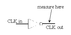
Part ONE (10 pts): Measuring Waveforms
If you don’t know how to use an oscilloscope, here is a good tutorial from Virginia Tech. This is for a different scope, but it’s close enough. Connect the power supply to the protoboard, but don't plug it in until you are done connecting up your experiment. It’s always a good idea to unplug the power whenever you are changing anything like plugging in chips, changing wiring, etc.
Connect power and ground to the portable clock generator in the kit, set the clock generator’s switches to give a 1MHz clock, insert the clock wire into the protoboard, and connect the clock signal to Vdd through a 4.7kOhm resistor (the bands for a 4.7k resistor are yellow, purple, red). Insert a 74LS04 inverter IC onto the protoboard, apply power and ground to the IC, put a 1µF capacitor across the power and ground pins of the IC, and drive the clock signal through one of the inverters to clean up the waveform. Tie the inputs to all the unused inverters to ground (to ensure that the outputs don’t oscillate). Measure the output waveform using an oscilloscope. Trigger the oscilloscope from the waveform itself.
- What is the clock frequency?
- What is the clock duty cycle?
- What are the logic 0 and logic 1 voltages (use averaging and cursors to measure these values)
- Measure the rise and fall times (20% – 80%, meaning from the point where the waveform has transitioned 20% of its total voltage swing to the point where it has transitioned 80%)? Do not eyeball these readings — use the oscilloscope’s cursors. Are the rise and fall times symmetric (rise same as fall)?
Part TWO (10 pts): Loading
Now rewire your circuit as shown. You will need to use a second SN74LS04.
Remember to connect it to ground and power.
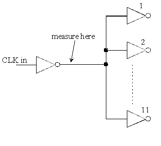
Measure the 20% – 80% rise and fall times for this configuration. If they
are different from the measurements you made on the 2-inverter circuit above,
explain why.
Part THREE (20 pts): Delays, Glitching, and Triggering
Assemble the LFSR shown below (LFSR stands for linear-feedback shift register. The circuit is also sometimes known as a pseudorandom noise generator). Use an SN74LS374, and connect four D flip flops in series as shown. Connect feedback into the first D flip-flop, using a 2-input XOR as shown. Connect power, ground, and clock (from the inverter output), and put 0.1µF capacitors across the power and ground pins of each IC.
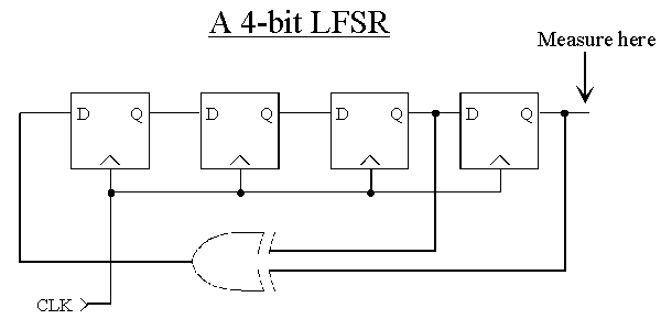
Using clock as an oscilloscope trigger, examine the circuit output. Can you see anything reasonable? If you see all 0s at the flip-flop outputs, short the input to the first flip-flop to Vdd momentarily, to start the LFSR. Now adjust the timebase, so you can see 16 bits on the screen. Why does the trace look like this? Try hitting the "single seq" button. Can you see anything now?
Now construct a 4-input AND gate to recognize the 4-bit pattern 1111 at the outputs of the 4 flip-flops. Use the data book to find a 4-input NAND or AND part. Put a decoupling capacitor across the power and ground of the IC. You may also need an inverter. If you construct your circuit properly, the AND will generate a pulse every 15 clock cycles. Trigger your oscilloscope using the output of this AND gate. Now do you see something reasonable at the LFSR output.
Measure the delay through the XOR. Is there any glitching at the XOR output? If so, explain why.
Look at the output of the 4th flip-flop. Record the 8 bit values that occur after the AND gate generates its pulse (i.e. after the falling edge of the AND pulse).