
Lab # 4
DUE: In one/two weeks, at 1:30 pm
Collaboration Policy:
Unless otherwise noted, your group may collaborate with
other CSE467 groups on the lab assignments. Collaboration means that you
may discuss the experiments and make notes during the discussion, but you
may not copy another groups work when doing the experiments; you may not
copy experimental results from another group; and you may not copy any
part of another groups lab report. In addition, every individual in a
group must understand the experiments, must participate in the writeup,
and should understand the results. Collaboration does not mean that one
person may perform the experiments and another write up the resultsall
lab partners must share equally in all parts of the lab assignment.
Late Policy:
The lab assignments are due as described in the schedule
(at the end of this document), at the beginning of your lab section. Assignments
handed in after lab will incur a 10% penalty; the penalty will increase
by 10% for each additional day late.
Overview:
The purpose of this lab is to give you experience using
Verilog to specify finite state machines. When you have completed this
lab, you will know how to:
The lab:
Answer all the questions in this handout in your lab
writeup. Show all of your work, and remember, your solutions must
be legible. This lab is worth 40 points.
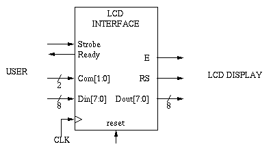
Part 1: Design an LCD Interface
In your DesignKit there is an LCD display that can display two lines of 16 characters each.
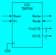
Part 2: Design an FSM to Write Your Name on the LCD Display
Design an FSM (called an LCD tester) that sends commands to your LCD interface, to write your name on the display. This FSM should have a reset and a go input. When go is asserted (use a debounced switch), the FSM should display your name and then quit. Reset should clear the display. Each team member should design their own FSM, that displays their name on the display.
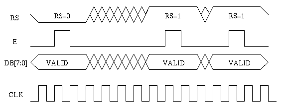
Your interface circuit converts a simple interface protocol to the somewhat more complicated protocol used by the LCD driver. The LCD accepts both instructions and data on its Din lines; whether it interprets the inputs as instructions or data depends on the value of the RS signal. For character write operations, set RS to 1. To execute a command, set RS to 0. The table below shows the instructions you will use. The first four instructions initialize the display for our configuration (a 1 line by 16 character display). Your LCD interface must issue these instructions whenever it resets.
Because you never need to read, you can tie the R/W control line directly to GND. The easiest way to write is to assert the enable signal (E) for one clock cycle during which both RS and data are stable. The signals that your LCD interface generates should look like:
You need to connect Vdd (+5V) and GND to the LCD display, and also connect the VO input to a potentiometer to provide a voltage between 0V and +5V. The potentiometer voltage sets the display contrast. We will give you the potentiometeryou will need to use a multimeter to figure out the terminals and how it works. The figure below (copied from the LCD documentation) shows how to make the connections.

A good part of designing a circuit is defining the problem. Most problem descriptions are incomplete or ambiguous. One of your tasks when designing is to turn an incomplete description into a precise specification. Before you begin the design, ask yourself what is missing and write down as precise a specification as you can. Hand in a written design specification along with your circuit design for this lab assignment.
NOTES:
2. The XESS board runs at 12MHz, which is too fast for the LCD display. The data sheet indicates that the display takes 40µs to execute a command (except for Home and Clear, which take 1.6ms). We could use counters to delay for ~400 cycles between issuing commands. Instead, we will divide down the FPGA clock so that it runs at 100kHz instead of 12MHz. Construct a 7-bit counter and connect the internal clock to the counter's high-order bit. Put this counter inside the FPGA. Put a BUFG on the counter output to buffer the internal clock signal. For the Home and Clear commands, you need to wait 1.6ms before asserting the Ready signal, so you will have to do some counting.
Divide each design into reasonably-sized components, such as registers and counters and combinational logic. Draw a top-level schematic for your design. You can use Verilog to specify both your sequential (e.g. FSM) and combinational (e.g. code converter) components. You can also use library and LogiBlox components.
You should simulate your circuit, and then download it to the XESS board. Use XESS board pins 8 and 9 for your input switches (reset and go) and pins 18, 19, 20, 23, 24, 25, 26, 27, 28, 29, 30 to connect to the LCD display. In addition, include the following connections in your top-level schematic. Doing so will disable the microcontroller on the XESS board so that it doesn't get in the way.

Schedule:
Turn in within one week: