CSE467 Homework 6


Distributed: February 25, 2005
Due: Start of Class, March 9, 2005


  1. [Pipelining and Retiming] Shown below is a filter circuit that generates a stream of outputs from a stream of inputs.  The block boxes are registers.  Assume the following delays:
    Add: 20
    Multiply: 50
    Register: 8 (setup time = 3, propagation delay = 5) corrected
    1. Examine all the cycles and find the greatest delay/register ratio.  This is the theoretically smallest clock period since a cycle can never lose or gain registers with pipelining or retiming.
    2. Use the pipelining and retiming rules to reach the smallest achievable clock period.  Show your process by applying one rule at a time (use this worksheet a just draw the registers).
    3. Can c-slowing be used to speed up the clock?  If so, demonstrate how.  If not, explain why.


  1. [Pipelining]  The figure below shows an abstract circuit where the ovals represent combinational logic whose min and max delays are given.  The registers all have the given parameters, where tsetup is the time before the clock edge that the value must be held for the register to latch it and tprop is the time it takes for the register’s output to change after the clock edge.
    1. What is the maximum clock rate for the circuit as shown?
    2. Can you pipeline this circuit to increase the clock rate?


  2. For each of the state diagrams shown below, complete the timing diagram at right. You may
    assume that all propagation delays are zero.

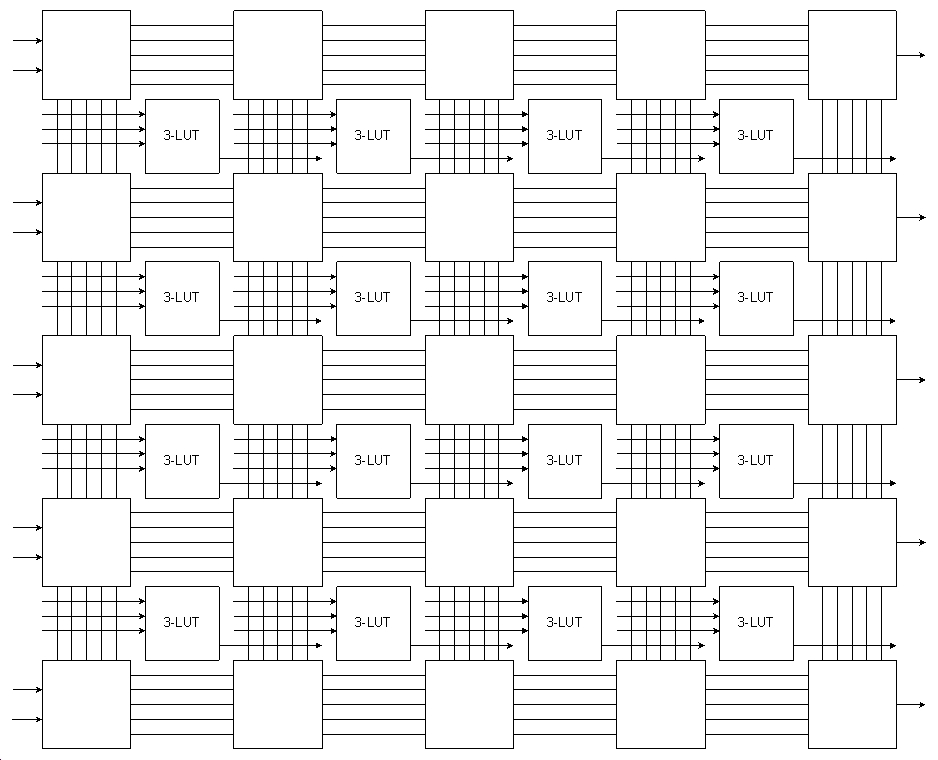
  3. Below is a simple FPGA architecture that uses 3-input LUTs.  Implement a 4-bit comparator, which compares two 4-bit unsigned numbers and produces a greater-than output, using this array.  Solve this problem using the following steps, showing all your work.  (Hint: you don’t need close to all the LUTs.)

    a) Factor the comparator function into a multi-level logic circuit, each node of which is a 3 (max) input function.  Name each of these functions using a letter that represents the output and give the function each computes.

    b) Place each of the functions from part a in the FPGA array by writing the name in the appropriate 3-LUT.

    c) Route the circuit together using the interconnection network.  Use an X to show the connection of each input and output of the 3-LUTs used.  Each of the switch boxes at the intersection of the row and column channels can connect each wire on one side to a wire on each of the other sides.  These connections can be made in either direction.  For each connection that you use in a switch box, draw an arrow to show the connection.  Circuit inputs arrive at the left and outputs leave at the right.(Here is the diagram you can print: fpga-worksheet.pdf)


Comments to: cgiefer@cs