UW CSE
Winter 2004
CSE467 Advanced Digital Systems Design
Lab # 4
DUE: In one week, at
Collaboration Policy:
Unless otherwise noted, your group may collaborate with other CSE467 groups on
the lab assignments. Collaboration means that you may discuss the experiments
and make notes during the discussion, but you may not copy another
group’s work when doing the experiments; you may not copy experimental
results from another group; and you may not copy any part of another
group’s lab report. In addition, every individual in a group must
understand the experiments, must participate in the writeup,
and should understand the results. Collaboration does not mean that one person
may perform the experiments and another write up the results – all lab partners
must share equally in all parts of the lab assignment.
Late Policy:
The lab assignments are due in one week, at the beginning of your lab section.
Assignments handed in after lab will incur a 10% penalty; the penalty will
increase by 10% for each additional day late.
Overview:
The goal of this lab is to start designing Verilog for sequential circuits and FSMs. In this lab, you will connect the keypad you used in the previous lab to an LCD display. As you press keys on the keypad, the corresponding character should be displayed on the LCD display. Time is now a factor because you need to determine when a key has been pressed and then send the appropriate commands to the LCD display to add a character to the display.
Part 1 – The Keypad Interface
The interface you designed last time simply converts a unary coding of the row and column to a binary coding for the key at that location. An extra Valid output indicates when a key is pressed. You will need to extend this interface to deal with the issue of switch bouncing. Switches are not ideal: as a switch makes or breaks a contact, there can be several transitions caused by the physical bouncing in the switch. Moreover, the connections for the row and column wires do not happen at exactly the same time. This means that the keypad interface must wait until both the row and column signals are asserted and stable before asserting the Valid output, and must wait until both row and column signals are unasserted and stable before de-asserting the Valid output.
One way to debounce switches is to filter the input signals by sampling them every T usec. and only letting the inputs pass through if (a) they are legal (e.g. a single row and a single column wire asserted) and (b) they have been the same for two consecutive samples. T is a value that depends on the switch and may require some experimentation. You can use the oscilloscope to watch how long the switches bounce, or you can make T a parameter that you adjust based on the operation of your circuit.
We will use the # key on the keypad to generate a system reset signal. This means that the keypad interface does not use a reset, so any FSM you design for this interface must be self-resetting. You should design and simulate your new keypad interface, but you will not be able to test your interface until you complete Part 2. You do not have to include the key-pair interface that recognizes when two keys have been pressed, i.e. Lab 3, Part 4.
Part 2 – LCD Interface
You will now add an LCD display to the protoboard in addition to the 7-segment displays. You will have to look at the LCD display datasheet to understand completely how it works, but we will be using only a small part of the functionality of this display. In particular, all you will need to do is:
1) Reset the display via a sequence of 4 commands.
2) Write a character to the display using a single command.
Start with the “Interface Pin Connections” table shown below from page 23 of the datasheet.
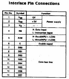
Pins 1-3 are power supply connections and will be explained later on. Pins 4-14 are signals that you must supply. RS and R/W are used to determine the operation being executed and E (enable) is used to provide a strobe that causes the operation to be executed. Since you will only be writing to the display, the R/W signal will always be 0. The data pins contain either an ASCII character code or a command code.
|
Operation |
RS |
DB7:0 |
|
Clear Display |
0 |
0000 0001 |
|
Function Set |
0 |
0011 0011 |
|
Display On |
0 |
0000 1100 |
|
Entry Mode Set |
0 |
0000 0110 |
|
Write Character |
1 |
DDDD DDDD |
Shown above is a table with the codes for the 5 commands that you need to execute. The first four should be executed in sequence on reset. The last command is used to write a character to the display. You can look at the documentation if you would like to try out other commands.
A timing diagram for sequencing the signals is shown at the top of page 37 of the datasheet. You will have to design an FSM to generate this timing. Note that the display does not run very fast. The Enable signal runs at a maximum of 1MHz, the Clear Display command requires several milliseconds to complete, and other commands take 40 usec. This means that your state machine will have to divide down the 50MHz FPGA clock to generate these signals with the right timing. There’s no reason to run the display fast – a 10KHz. rate should work fine. By the way, you can either divide the system clock down to a slow clock that runs the display, or use a counter in the display interface to sequence between states in the interface FSM. You should think about how you might use the same slow clock for both the keypad and the display.
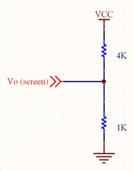
You should now wire the LCD interface into the FPGA board. GND should be connected as usual, but Vdd should be connected to the +5v output of the FPGA board. In addition, you will need to set the contrast for the LCD screen. For this, we have to apply a voltage at the Vo pin that we can obtain using the voltage divider circuit shown in the figure below. This circuit will generate a voltage for Vo of approximately 1/(1+4) of VCC or .2 of 5 volts or 1 volt. Look at the Interface Pin Connections table to find the location of the Vo pin. In your kit should be a 3.9K ohm resistor and a 1K ohm resistor. You can determine the resistance value of a resistor by the color coded bands on the resistor (see explanation of how the color coded system works and an automated calculator).
Part 3 – Testing
Combine your keypad circuit with your LCD interface circuit, compile, download and test on the FPGA. You may have to adjust your T value to make your keypad interface robust.
Turn in your Verilog programs, any schematics and simulation files you use. Demo your design and have the TA sign off on the programs that you turn in.