Building our Hack CPU
You are encouraged to post any questions about the reading on the course discussion board!
We've spent a little time exploring the Hack assembly language, which details the types of instructions we can execute on our CPU. This reading will start the complicated process of learning how to implement the logic in the CPU that allows us to execute those instructions. Specifically, we will discuss a high-level organization of our CPU including what sub-chips we will use to implement it.
Using our instruction types to inform our CPU design
Remember that our CPU needs to be able to execute the two types of instructions in our Hack assembly language: A-instructions and C-instructions. We will use the behavior of these instructions that we learned about last week to inform what we need to include in our CPU design. Roughly, we will cover the following tasks:
- A-instructions
- Need to be able to load values specified with the
@valuesyntax
- Need to be able to load values specified with the
- C-instructions
- Need to be able to perform different computations
- Need to be able to store the result of those computations in different destinations
- Flow Control
- Need to keep track of our current address and know what address to execute next
Chips we know we will need
There are a few chips we know we will need for our CPU implementation. Here's a list of these core components:
A Register: For storing values in our A registerD Register: For storing values in our D registerALU: For performing computationsProgram Counter (PC): For keeping track of flow control
The tricky part will be figuring out how to wire these together and build the circuits that control the logic for these components.
High Level Design
Here we provide a high-level design similar to the one mentioned in the textbook. The following sections will walkthrough how exactly we determined each portion of these designs based on our instruction functionality.
In this design, there is still a lot of logic that has yet to be implemented. Anywhere you see an arrow with c as the input, this signifies logic that you will implement as part of project 5. You'll notice that we've given you a rough design of how the core components fit together, and your job is to figure out the details of the logic associated with the various components.
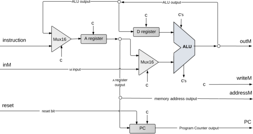
A-instruction Design
Here is the portion of the diagram related to the A-instructions:
How did we come up with this design? It should be pretty straightforward why we would want the instruction to be fed into the A Register. In the case of an A instruction, we want to load the value of the instruction into the A Register.
So why all the nonsense with the Mux/previous ALU output? If you reference the possible destinations of a C-instruction, you'll notice that one possible destination for the computation's result is the A Register! So we need to be able to route either the instruction value or the output of the computation to the A Register depending on the instruction type, which is why we have the Mux16 to choose between those two options.
C-instruction Design
Here is the portion of the diagram relating to C-instructions (you can see it's most of the diagram):
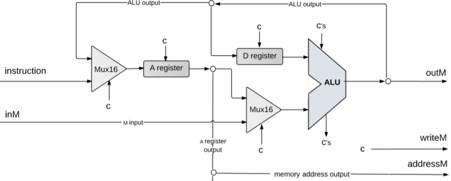
We break down this diagram into three components: inputs, computations, and destinations.
Inputs
The first part of the C-instruction is determining where the inputs come from. If you examine the range of possible computations, you'll notice that we need to be able to retrieve values from the following locations:
- The
D register - The
A register - A value in memory (the
M register)
You'll also notice we have the following combinations of the above registers:
- Computations involving only one of the three registers
- Computations involving both the
D registerand theA register - Computations involving both the
D registerand a value in memory (theM register)
You'll note that the A register and the value in memory (the M register) never are involved in a computation together! This hints as to why we can have them share one of the inputs to the ALU using a Mux16 - we only need one or the other (never both).
For our other input, we can just always have it use the output of the D register. What about constants you might ask? Remember that the ALU generates constants using the control bits of the instruction, so we don't need to worry about feeding the constants to the ALU (just the appropriate control bits).
Computations
Now that we've determined where the inputs come from, how do we know what to compute? It turns out that your instruction has bits that are used to determine what computation is performed! If you look at the specification for the compute field in Chapter 5, you'll see that these are very similar to the control bits specification given for our ALU. All we have to do is pass these along to tell the ALU what to compute with the given inputs.
Destinations
Now that we've computed a value, we have to determine where that value should be used. There are three destinations that can be specified in our Hack assembly language: the A register, the D register, and a location in memory (the M register). Notice how our output from the ALU is routed to each of these three locations! It circles back around to the Mux16 that feeds the A register and the D register, and it is also connected to the outM output from the CPU! The addressM output works with the outM output such that the Memory chip knows which address to update with the value (notice how addressM is fed the output of the A register).
One thing to note is that the ALU output is only loaded to each of these locations sometimes. For the location in memory (the M register), outM will only be written to addressM if writeM is true. For the A register and D register, there is a load signal that must be true in order to update their values. Your job in project 5 will be to use the destination bits of the instruction to determine when each of these locations should be updated with the ALU output.
Flow Control Logic
Our last piece of the diagram is the portion related to flow control logic. Here's the full diagram again:
The reset pin and output are fairly straighforward. We want to reset the Program Counter any time the CPU's reset is triggered. The Program Counter output is fed to the CPU's PC output, which will be used to fetch the next instruction to execute.
Notice how the input to the Program Counter is the output of the A register. Remember that the input to the Program Counter is loaded if the load signal is true. If you also recall that when we execute a jump instruction in our Hack assembly language, we jump to the address in the A register. Now the choice of our input to the Program Counter should make sense! We feed it the A register's output because that is that value we want to load in the case that we jump.
The control bits for the Program Counter are not shown in detail in our diagram. Remember that there are two things that determine if a jump occurs: the jump condition, and the output of our computation. We can get infomration about the jump condition from the jump bits in the instruction, and we can get information about the output of our computation from the status flags in the ALU!
The Road Ahead
Wow, that was a lot of information! In lecture we will build off of this information and start to discuss how you can determine the logic for the control bits that need to be implemented. This will set you up to be able to build a fully functioning, virtual computer in project 5!