LabsLand Breadboard GPIO Guide
GPIO on the DE1-SoC
The DE1-SoC has two General Purpose Input/Output ports
(GPIO_0 and GPIO_1) with expansion
headers (2 × 20 = 40 pins total) that are used to connect
peripherals to the board.
On LabsLand, these are controlled using the V_GPIO.
The GPIO pin assignments are already defined in a .qsf
file (generated by Quartus) so you can add them to your top-level
SystemVerilog module in the same way as switches and LEDs.
/* This example shows how to control a LED on the breadboard using a switch
* on the breadboard. The components on the breadboard are wired according
* to Step 5. Specifically, V_GPIO[24] (JP1 pin #24) is connected to
* a switch and V_GPIO[35] (JP1 pin #35) is connected to an LED.
*/
module GPIO_example (V_GPIO);
// SW and KEY cannot be declared if V_GPIO is declared on LabsLand
inout logic [35:0] V_GPIO;
// Assign V_GPIO[35] (LED) to V_GPIO[24] (switch)
assign V_GPIO[35] = V_GPIO[24];
endmodule // GPIO_example
/* Test bench for the GPIO example module */
module GPIO_example_tb ();
// inout pins must be connected to a wire type
wire [35:0] V_GPIO;
// additional logic required to simulate inout pins
logic [35:0] V_GPIO_in;
logic [35:0] V_GPIO_dir; // 1 = input, 0 = output
// set up tristate buffers for inout pins
genvar i;
generate
for (i = 0; i < 36; i++) begin : gpio
assign V_GPIO[i] = V_GPIO_dir[i] ? V_GPIO_in[i] : 1'bZ;
end
endgenerate
GPIO_example dut (.V_GPIO);
initial begin
// you only need to set the pin directions once
V_GPIO_dir[24] = 1'b1;
V_GPIO_dir[35] = 1'b0;
// manipulate the V_GPIO input bits indirectly through V_GPIO_in
V_GPIO_in[24] = 1'b1; #50;
V_GPIO_in[24] = 1'b0; #50;
end
endmodule // GPIO_example_tb
Virtual Breadboard on LabsLand
- Log into your LabLands account (please refer to LabsLand setup for an account).
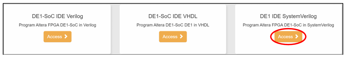
- Navigate to the SystemVerilog IDE:
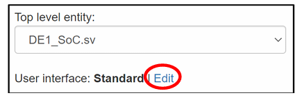
- Locate the "User interface" heading above the Documentation box
and click "Edit" next to it:
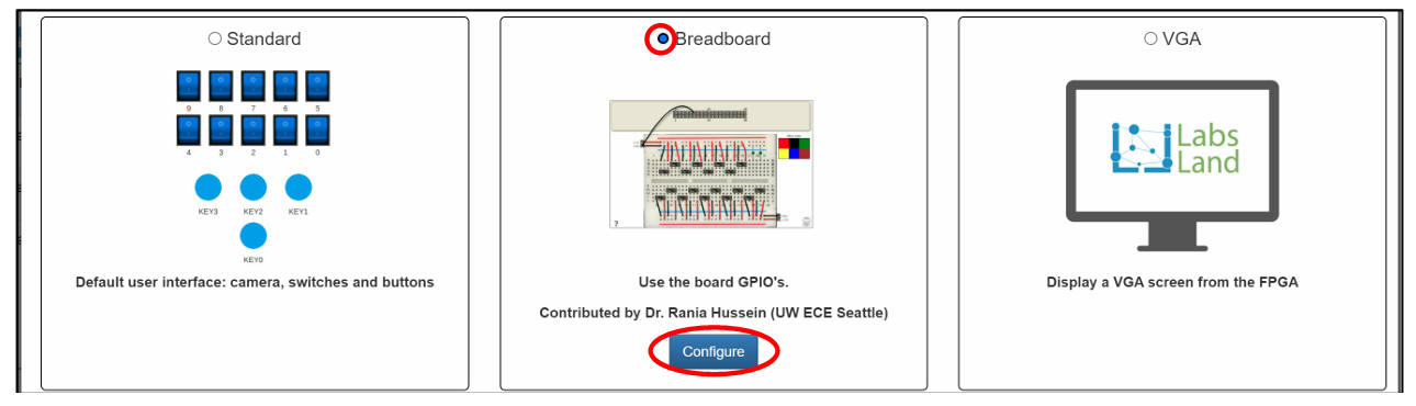
- In the resulting pop-up window, select the "Breadboard" option and
click the "Configure" button under the "Breadboard" tile:
- You will be directed to the following setup window,
where you can connect circuit components that are available on the
breadboard (switches and LEDs) to the GPIOs.
The right side shows the relationship between GPIO and JP1.
The left side is the actual configurator you will use to connect
wires between the GPIO and the circuit components:
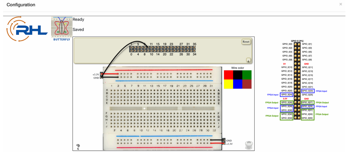
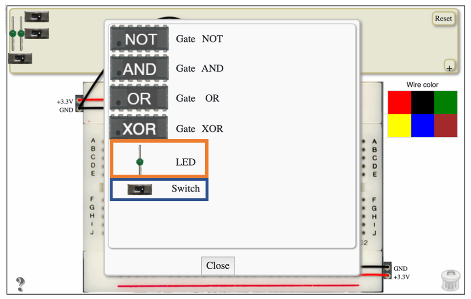
- Click on the "+" button on the right to bring about a list of
available breadboard supported components. Here, the ones to take
note are the switches and LEDs. Click on the components to add it
to the top left corner of the breadboard.
- Click on each component on the top left corner of the breadboard and drag them to the desired locations on the breadboard.
- Click on a wire color on the right to turn your mouse into a wire-
drawing pen. Then click and hold your mouse to draw a cable
connecting the GPIO header and the breadboard. Repeat the process
to create all the wires for your design.
Note: Pay attention to the FPGA Inputs and Outputs image when connecting the switches and LEDs to the 40-pin connector. You can only connect switches to FPGA Inputs, and can only connect LEDs to FPGA Outputs.
- For switches: Wire the switch connections such that the left
side connects to +3.3V, and the right side connects to GND.
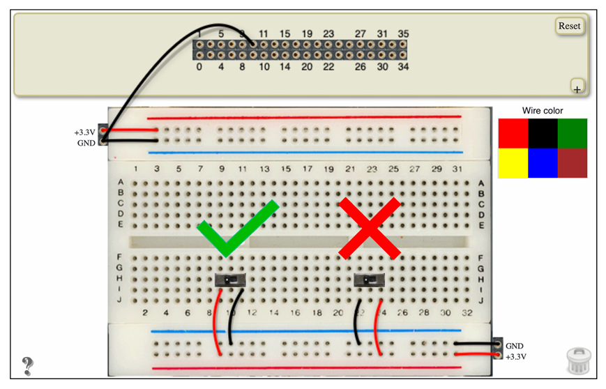
- For LEDs: Place one end of the LED to a GND breadboard node.
- For switches: Wire the switch connections such that the left
side connects to +3.3V, and the right side connects to GND.
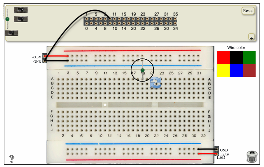
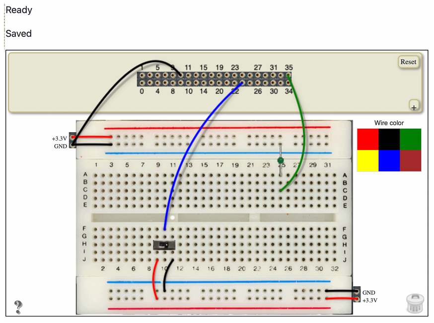
- For the sample code in Figure 1, you will want a configuration similar to the one shown below: JP1 pin 24 can be connected to the middle pin of your virtual switch and JP1 pin 35 can be connected to your virtual LED:
- Click on the "+" button on the right to bring about a list of
available breadboard supported components. Here, the ones to take
note are the switches and LEDs. Click on the components to add it
to the top left corner of the breadboard.
- When you are done wiring your breadboard, make sure that the message above the breadboard says "Saved". Press the "Close" button to leave the configurator. Once you send the code to the FPGA, you will see the breadboard exactly as you saved it in the breadboard configurator!
- To change your virtual switch states, press and hold on the switch image, or double click. A single click brings up a circle element surrounding the component, used to drag the component to a different location on the breadboard, or to delete that component.
Common Virtual Breadboard Error Messages and Solutions
- "Ready" — No errors found in your breadboard design.
- "Error: A virtual switch is not properly wired" — Take a look at the wiring of your switches. The left side should connect to +3.3V. The right side should connect to GND. The middle should connect to a "FPGA Input" GPIO pin.
- "Error: A virtual LED is not properly wired" — Take a look at the wiring of your LEDs. Drag the LED to a position on the breadboard such that one side of that LED is connected to a GND horizontal node. The other side of the LED must be connected to a "FPGA Output" GPIO pin.
- "Error: Both ends of a wire are connected to an input" — Take a look at your breadboard wirings. For an LED, one end must be connected to a "FPGA Output" GPIO pin. For a switch, the middle switch connection must be connected to a "FPGA Input" GPIO pin.
- "Error: Both ends of a wire are connected to an output" — Take a look at your breadboard wirings. For an LED, one end must be connected to a "FPGA Output" GPIO pin. For a switch, the middle switch connection must be connected to a "FPGA Input" GPIO pin.
- "Error: Every wire must be connected to a valid component or valid GPIO" — Take a look at your breadboard wirings. Every end of a wire must be connected to a component (switch or LED) or to either an FPGA Input or FPGA Output connection.