Lab 4: Implementing Algorithms in Hardware
Out: Thursday, April 23, 2026
Due: Friday, May 8, 2026 by 11:59 PM
Closes: Sunday, May 10, 2026 by 11:59 PM
Demos: Friday, May 15, 2026 by end of last office hour
Overview
In this lab, you will use Algorithmic State Machine with Datapath (ASMD) charts to implement algorithms as hardware circuits.
ASMD Review
The implementation of algorithms in hardware is often performed by separating the data storage and manipulation components (the datapath circuit) from an FSM for the routing logic (the control circuit).
A key distinction between ASMD charts and flow charts is a concept known as implied timing. The implied timing specifies that all actions associated with the current state (i.e., the active path in the ASM block) take place only when the next active clock edge occurs. For a more thorough review of ASMD charts, see the lecture slides.
Lab Code
For .sv files, you may want to right-click and save/download instead of clicking.
- seg7.sv (same as Lab 2)
Instructions
Task 1 – Bit-Counting Algorithm
The ASMD chart shown in Figure 1 represents a circuit that counts the
number of bits set to 1 in an n-bit input A
(i.e., A =
an-1an-2…a1a0).
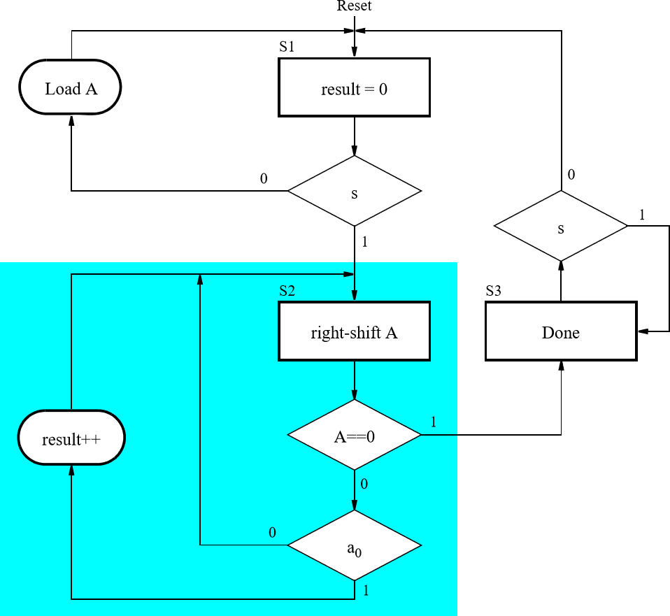
Implement the bit-counting circuit given by the ASMD chart in Figure 1 in SystemVerilog to run on the DE1-SoC, combining the necessary datapath components and a control circuit FSM.
- The inputs to your circuit should consist of an 8-bit input
(
A) connected to switchesSW7–SW0, a synchronous reset connected toKEY0, and a start signal (s) connected toKEY3. - Use the 50 MHz clock signal provided on the
DE1-SoC as the clock input for your circuit.
Be sure to handle metastability properly in your
sinput. - Display the number of
1's counted inAon the 7-segment displayHEX0, and signal that the algorithm is finished by lighting upLEDR9.
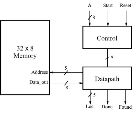
Task 2 – Binary Search Algorithm
Implement a binary search algorithm, which searches through an
unsigned array to locate an 8-bit value A once
the user presses Start.
A block diagram for the circuit is shown in Figure 2.
The binary search algorithm works on a sorted array. Rather than comparing each value in the array to the one being sought, we first look at the middle element and compare the sought value to the middle element. If the middle element has a greater value, then we know that the value we seek would be in the first half of the array. Otherwise, the value we seek would be in the second half of the array. By applying this approach recursively, we can complete our search in many fewer steps.
logic is an unsigned data type in
SystemVerilog (i.e., the stored bits are interpreted by
their non-negative binary value).
Comparisons such as > and < are
unsigned comparisons on logic values,
regardless of what radix you are using to display their value in
ModelSim.
For example, if logic [7:0] x = 8'd2;, it turns out
that x > -1 returns false, because -1
is stored as 8'hFF, which is interpreted as
255 in unsigned.
System Specifications
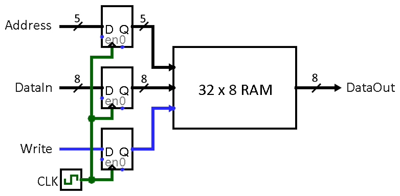
- The array, which you can assume has a fixed size of 32 elements, is stored in a memory module that is implemented inside the FPGA. A diagram of the memory module that we need to create is depicted in Figure 3. This memory should contain a sorted collection of 8-bit unsigned integers.
- Inputs:
Ashould be specified on switchesSW7–SW0,StartonKEY3, andResetonKEY0. - Outputs: 5-bit output
Loc, which specifies the address in the memory where the numberAis located, a signalDoneindicating that the algorithm is finished, and a signalFoundthat should be high ifAwas found and low otherwise.- Display
Loc, if found, in hex onHEX1–HEX0,DoneonLEDR9, andFoundonLEDR0.
- Display
Step-by-step Instructions
- Create an ASMD chart for the binary search algorithm. Keep in mind that the memory has registers on its input ports – when would you expect to see the output associated with new inputs?
- Implement the control FSM and the datapath for your circuit as separate modules.
- Create a memory that is eight-bits wide and 32
words deep in a similar fashion to Lab 2 Task 1 and then connect it
to your FSM and datapath as indicated in Figure 2.
Use the DE1-SoC's 50 MHz clock signal as the
Clockinput and be sure to synchronize theStartinput to the clock (i.e., handle metastability). - Create a memory initialization file called my_array.mif (refer to Lab 2 Task 3 Step 2) and fill it with an ordered set of 8-bit unsigned integers of your choice. Make sure that this file is saved in the same folder as the Quartus project.
- Make sure that your design works in simulation and on the DE1-SoC.
- After you have Tasks 1 and 2 working, add the
ability to switch between them in the same program using
SW9.
Lab Requirements
Lab Report
Due by the end of Friday, submitted as a PDF on Gradescope.
- Include the required Design Procedure, Results, and
Experience Report sections along with the other requirements
listed in the
Assignment Requirements.
- Notice that Figure 1 does not currently include your control signals or ASM blocks. Also notice that Figure 2 does not currently include your control or status signals.
- As separate files, upload your commented code files (.sv and generated .v), including test benches.
Lab Demo
Due within one week of the lab report deadline, but typically during your assigned demo slot or a scheduled office hour.
- Demonstrate your working Task 1 bit-counting algorithm on different inputs.
- Explain what your Task 1 reset signal does in your code.
- Show your Task 2 memory initialization file to the TA so they know the contents of the memory.
- Demonstrate your working Task 2 binary search algorithm for found and not found inputs.
- Explain what your Task 2 reset signal does in your code.
- Be prepared to answer 1-2 questions about your lab experience to the TA.