HW1: FSM and SystemVerilog Review
Out: Tuesday, March 31, 2026
Due: Monday, April 6, 2026 by 11:59 PM
Closes: Tuesday, April 7, 2026 by 11:59 PM
Homework Files
Starting a Project
You can (1) start from a copy of an existing project folder from EE 271 or CSE 369 or (2) watch the following video on how to create a Quartus project from scratch [YouTube].
Helpful Project Files
The use of these are optional, depending on your preferred workflow. Versions of these should have been provided in EE 271 and CSE 369.
- Launch_ModelSim.bat (to launch ModelSim from the directory instead of through Quartus)
- runlab.do (to script the ModelSim commands for simulation)
Code for this Homework
For .sv files, you may want to right-click and save/download instead of clicking.
- hw1p1.sv
- hw1p1_tb.sv
- fullAdder.sv (optional to use on Problem 1)
- fullAdder_tb.sv (optional to use on Problem 1)
- hw1p2.sv
- hw1p2_tb.sv
Problems
Problem 1
A sequential circuit has two inputs, x and y, and one output, S. It consists of a full-adder circuit connected to a D flip-flop, as shown in the following diagram.
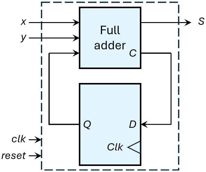
- Draw out the state diagram of this circuit. Don't forget a reset state.
- Implement modules hw1p1 and
hw1p1_tb, which thoroughly simulates an instance
of hw1p1 called/named dut.
- Make sure that hw1p1 contains intermediate signals Q and C.
- Use the names clk and reset (all lowercase) for your clock and reset signals.
- Only light code commenting required; you are expected to simulate and verify your design, but do not need to provide a waveform screenshot or explanation in your submission PDF.
Problem 2
The state diagram shown describes a Mealy finite state machine.
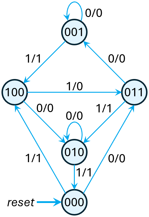
- Implement modules hw1p2 and
hw1p2_tb, which thoroughly simulates an instance
of hw1p2 called/named dut.
- Make sure to use both ps and ns as state signals.
- Use the names clk and reset (all lowercase) for your clock and reset signals and in and out for your input and output signals.
- Only light code commenting required; you are expected to simulate and verify your design, but do not need to provide a waveform screenshot or explanation in your submission PDF.
Problem 3
This SystemVerilog code describes a finite state machine.
- Draw out the state diagram for the FSM.
input logic clk, reset, a, b;
output logic y;
enum logic [1:0] {S0, S1, S2, S3} state, nextstate;
always_ff @(posedge clk, posedge reset)
if (reset) state <= S0;
else state <= nextstate;
always_comb
case (state)
S0: if (a ^ b) nextstate = S1;
else nextstate = S0;
S1: if (a & b) nextstate = S2;
else nextstate = S0;
S2: if (a | b) nextstate = S3;
else nextstate = S0;
S3: if (a | b) nextstate = S3;
else nextstate = S0;
endcase
assign y = (state == S1) | (state == S2);
endmodule // fsm
Problem 4
Consider the functionality of the following two SystemVerilog modules.
- Sketch the hardware each one implies. Then replace every <= assignment with = in both modules and sketch the new hardware that each one implies.
- Your submission should cover four situations in total.
input logic clk, a, b, c;
output logic y;
logic x;
always_ff @(posedge clk) begin
x <= a & b;
y <= x | c;
end // always_ff
endmodule // circuit1
input logic clk, a, b, c;
output logic y;
logic x;
always_ff @(posedge clk) begin
y <= x | c;
x <= a & b;
end // always_ff
endmodule // circuit2
Submission Requirements
Due by the end of the deadline day, submit your solutions (e.g., text, diagrams, screenshots, work) as a single PDF file ending in .pdf (all lowercase) to Gradescope.
- Include the requirements listed in the Assignment Requirements.
- At the end of your document, estimate how long you
spent working on the homework and rate the difficulty on the
following scale:
Very Hard — Hard — Moderate — Easy — Very Easy - As separate files, upload your commented
SystemVerilog files (.sv), including test benches.
- hw1p1.sv
- hw1p1_tb.sv
- fullAdder.sv (if you used it)
- hw1p2.sv
- hw1p2_tb.sv
Grading Rubric
- FSM diagram
- Implementation and Simulation
- Implementation and Simulation
- FSM diagram