Lab 3: Digital Signal Processing
Overview
In this lab, you will use the audio coder/decoder (CODEC) on the DE1-SoC to generate and filter noise from both an external source and an internal memory.
Audio Signals
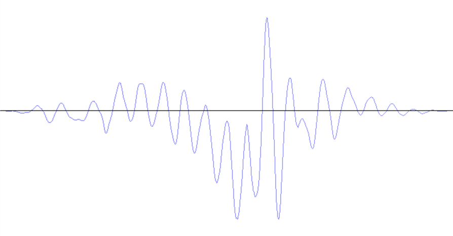
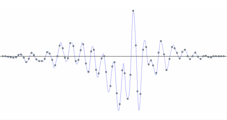
Sounds, such as speech and music, are signals that change over time. The amplitude of a signal determines the volume at which we hear it. The way the signal changes over time determines the type of sounds we hear. For example, an "ah" sound is represented by a waveform shown in Figure 1. The waveform is an analog signal, which can be stored in a digital form by using a relatively small number of samples that represent the analog values at certain points in time. The process of producing such digital signals is called sampling. The points in Figure 2 provide a sampled waveform. All points are spaced equally in time and they trace the original waveform.
|
|
The DE1-SoC Audio CODEC
The DE1-SoC is equipped with an audio CODEC capable of sampling sound from a microphone and providing it as an input to a circuit. By default, the CODEC provides 48000 samples per second (48 kHz), which is sufficient to accurately represent audible sounds (by the Nyquist-Shannon sampling theorem).
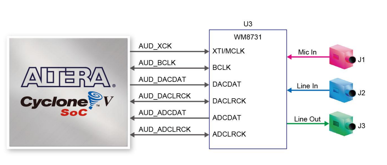
To simplify this lab, a system that can record and play back sounds on the board is provided as a "starter kit." The system comprises a Clock Generator, an Audio CODEC Interface, and an Audio/Video Configuration module (Figure 4). For this lab, we will assume that our audio will be split into two channels, left and right, that are intended to be played from multiple speakers (e.g., left and right earbuds/headphones).
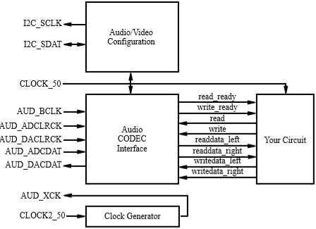
The left column of signals in Figure 4 are the inputs and outputs of the system. These I/O ports supply the clock inputs and connect the Audio CODEC and Audio/Video Configuration modules to the corresponding peripheral devices on the DE1-SoC. The right column of signals connects the Audio CODEC Interface module to your circuit and allows your circuit to record sounds from a microphone and play them back via speakers.
Audio CODEC System Interface
- Upon reset, the Audio/Video Configuration begins an auto-initialization sequence. The sequence sets up the audio device to sample microphone input at a rate of 48 kHz and produce output through the speakers at the same rate.
- Once the auto-initialization is complete, the Audio CODEC begins reading the data from the microphone once every 48,000-th of a second and sends it to the Audio CODEC Interface core in the system. Note that this is significantly SLOWER than the DE1-SoC's onboard 50 MHz clocks.
- Once received, a sample is stored in a 128-element
buffer in the Audio CODEC Interface core.
The first element of the buffer is always visible on the
readdata_leftandreaddata_rightoutputs (i.e., 2 channels for 1 sample), but the data is only valid when theread_readysignal is asserted. When you assert thereadsignal, the current sample is replaced by the next element one or more clock cycles later, indicated byread_readybeing reasserted. - The procedure to output sound through the speakers
is similar.
Your circuit should monitor the
write_readysignal. Only when the Audio CODEC is ready for a write operation should your circuit assert thewritesignal to write a sample from thewritedata_leftandwritedata_rightsignals. This operation stores a sample in a buffer inside of the Audio CODEC Interface, which will then send the sample to the speakers at the right time.
Instructions
Task 1 – Passing Music Through the FPGA
In this task, you will play a music file into the audio input of the DE1-SoC, which will simultaneously be played through the audio output of the device.
- Modify the provided starter kit circuit to pass the audio input to audio output only when the CODEC is ready. Hint: BOTH the audio input and audio output have to be ready for data passing!
- In LabsLand, upload an audio file (either the provided piano_noisy.mp3 (code) or your own – see the for restrictions) alongside your synthesized circuit and verify that the preview of the audio file matches your recorded output sample. Recall that in LabsLand, you must record while playing the audio file into the DE1-SoC.
read and
write signals.
Task 2 – Play a Tone from Memory
In this task, you will produce a static tone from memory. By storing the samples from a sound's waveform, you can play back those samples later to re-produce the sound. We have provided a Python script (code) which generates MIF files for a desired tone, which can then be loaded into memory. Information on how to use this Python script can be found in .
- Follow the tutorial on using the python script to create a MIF
file with your desired tone.
Create a ROM that initializes to the values stored in the MIF file
using Quartus' built in library modules:
- Open the IP Catalog in the Quartus menu by clicking on Tools → "IP Catalog". In the IP Catalog window, expand "Library", then "Basic Functions", then "On Chip Memory". Then double-click "ROM: 1-PORT".
- Give the file an appropriate name, select "Verilog" as the file type, then click "OK" to open the configuration wizard.
- In the first window, specify 24-bits as the word width. You will need to check your generated MIF file to find the number of words, as this will vary. Select "M10K" for memory block type and "Single clock" for the clocking method, then click "Next >".
- Click "Next >" past the "Regs/Clken/Aclrs" window, keeping the default selections.
- In the next window, under "Do you want to specify the initial contents of memory?", select "Yes, use this file for the memory content data" and specify your MIF file. Click "Finish" to use the rest of the default settings, then click "Finish" again at the summary page to exit the wizard. If prompted, add the new Quartus Prime IP File to your project by clicking "Yes".
- Output the values stored in your ROM sequentially to the Audio CODEC, looping back to the start when you reach the end. Make sure to increment the address only once each time you write.
- Compile and download your overall design to the DE1-SoC, record the generated tone in LabsLand, and then listen to the generated tone played from the FPGA.
- Combine your Task 1 and Task 2 by instantiating
them in a single top-level module that plays the input audio (Task
1) when
SW9=0and your tone from memory (Task 2) whenSW9=1. While testing, you should switch between the tasks about halfway through your recording.
Task 3 – FIR Filter
In this task, you will learn a basic signal processing technique known as filtering. Filtering is a process of adjusting a signal (e.g., removing noise). Noise in a sound waveform is represented by small, but frequent changes to the amplitude of the signal.
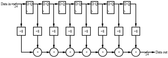
A simple logic circuit that achieves the task of noise-filtering is an averaging Finite Impulse Response (FIR) filter. An averaging filter removes noise from a sound by averaging the values of adjacent samples. Conceptually, a basic FIR filter uses registers as delay blocks and computes the moving average from their outputs, as shown in Figure 5.
However, we can achieve the same result using a FIFO buffer and accumulator (i.e., a register whose input is the sum of the next incoming data value and its current stored value), as shown in Figure 6.
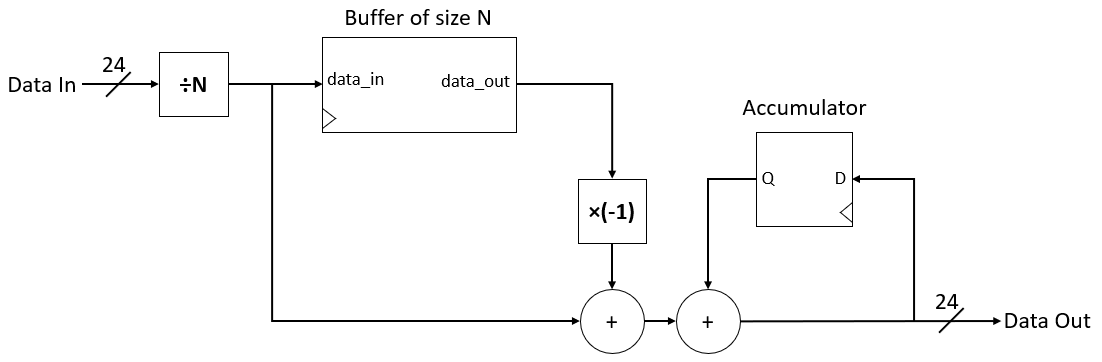
To compute the average of the last N samples, this circuit first divides the input sample by N. Then, the resulting value is stored in a First-In First-Out (FIFO) buffer of length N and added to the accumulator. To make sure the value in the accumulator is the average of the last N samples, the circuit subtracts the value that comes out of the FIFO, which represents the (N+1)th sample.
wire and
logic are, by default, unsigned data types but
we are using them for signed arithmetic:
- The most robust way to divide by a power of two
is using an arithmetic right shift.
The following code snippet uses the replication and concatenation
operators to divide the w-bit signal data by
2n:
assign divided = {{n{data[w-1]}}, data[w-1:n]}; - Please pay attention to Figure 6 and make sure
that you are adding
data_outmultiplied by -1 instead of subtracting.
- Although the starter kit includes an Altera library FIFO buffer, we recommend using the circular queue implementation from lecture and hw3 for familiarity and ease of use.
- Carefully consider how to ensure that your FIR filter updates when it is supposed to. As a single system, the FIFO buffer and accumulator should be synchronized together (i.e., at any clock trigger, either BOTH or NEITHER should update). But when should they update based on the CODEC signals?
- The description below Figure 6 is accurate once the FIFO buffer is full. However, you should carefully consider what your buffer will do while the first N-1 samples are read (i.e., at the beginning or after a reset) and make sure that the value of the accumulator also matches the buffer behavior during this time period.
- Implement the N-sample averaging FIR filter.
Use
SW8to select between filtered (SW8=1) and unfiltered (SW8=0) audio to output; this filtering should be able to interact with both Task 1 (SW9=0) and Task 2 (SW9=1). - Compile and download your overall design on LabsLand and use piano_noisy.mp3 to generate your recorded output.
- Experiment with different
values of N to see what happens to the noisy audio sample.
Use the switch to tell what kind of effect the filter is having on
the audio.
- When you change N, remember to adjust both the FIFO buffer length and the circuit divisor. We recommend experimenting with values of N that are powers of 2 for easier division.
Lab Requirements
Lab Report
Due by the end of Friday, submitted as a PDF on .
- Include the required Design Procedure, Results, and
Experience Report sections along with the other requirements
listed in the
.
- You only need to include simulations for modules you have written, you can assume all of the provided files work without simulation.
- Task 1: The design can be a short description and/or a small circuit diagram. No simulation needed.
- You should omit top-level simulations for this lab, as
mimicking the
AUDandI2Csignals is unreasonable. However, you should still include a top-level block diagram and description. Do NOT just include Figure 4 – we need to see/know what happens in "Your Circuit"!
- As separate files, upload your commented code files (.sv and generated .v), including test benches.
Lab Demo
Due within one week of the lab report deadline, but typically during your assigned demo slot or a scheduled office hour.
- Demonstrate all working Tasks using
SW9andSW8, with your FIR filter size N set to the "best" length that you found. You will need piano_noisy.mp3 uploaded. - Briefly walk your TA through your N-sample averaging FIR filter SystemVerilog file.
- Be prepared to answer 1-2 questions about your lab experience to the TA.
Grading Rubric
- Do discuss Task 1, but explicit diagram may be unnecessary; include and discuss designs for ROM and FIR filter modules
- Top-level block diagram can build off of Figure 4 but should include connections between your defined modules
- No simulations needed for provided/reused modules, Task 1, or top-level module