Lab 2: Memory Blocks
Overview
In computer systems, it is necessary to provide a substantial amount of memory. If a system is implemented using only FPGA technology, it is possible to provide some amount of memory by using the memory resources that exist in the FPGA device. In this lab, we will examine the general issues involved in implementing such memory.
The FPGA included on the DE1-SoC board provides dedicated memory resources and has M10K blocks, each of which contains 10240 memory bits. The M10K blocks can be configured to implement memories of various sizes. A common term used to specify the size of a memory is its aspect ratio, which gives the depth (in words) and the width (in bits) as depth × width. In this lab, we will use an aspect ratio of 32 × 3.
There are two important features of the M10K blocks:
- They include registers to synchronize all the input and output signals to a clock input.
- They have separate ports for writing data to the memory and reading data from the memory.
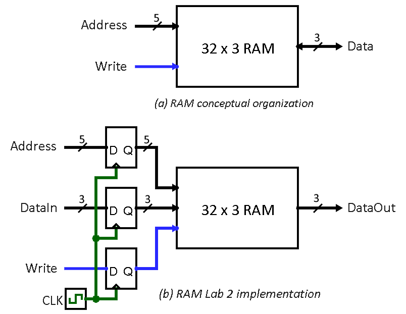
A conceptual diagram of the Random-Access Memory (RAM) module that we want implement is shown in Figure 1a. It contains 32 three-bit words (i.e., rows) that are accessed using a five-bit Address port, a three-bit bidirectional Data port, and a Write control input. However, given the properties of the M10K blocks, we will instead implement the modified 32 x 3 RAM module shown in Figure 1b. It includes registers for the address, data input, and write ports, and uses a separate unregistered data output port.
Instructions
Task 1 – Memory Using Library Modules
Commonly used logic structures, such as adders, registers, counters, and memories, can be implemented in an FPGA chip by using prebuilt modules that are provided in libraries. In this task, we will use such a module to implement the memory shown in Figure 1b.
- Create a new Quartus project.
- Get a library RAM module from the IP Catalog:
- Open the IP Catalog in the Quartus menu by clicking on Tools → "IP Catalog".
- In the IP Catalog window, expand "Library", then "Basic Functions", then "On Chip Memory". Then double-click "RAM: 1-PORT".
- In the "Save IP Variation" dialog box that opens, append the text "ram32x3.v" to the end of the file name and select "Verilog" as the file type. Then click "OK" to open the configuration wizard.
- In the configuration window, specify 3-bit width for the output bus and 32 words of memory. Then select the "M10K" radio button for memory block type and "Single clock" for the clocking method before clicking "Next >".
- Now, deselect the check box for registering (i.e., placing a register on) the "'q' output port". This creates a RAM module that matches the structure in Figure 1b. Click "Finish" to accept the defaults for the rest of the settings in the Wizard.
- You will have to click "Finish" one more time at the Summary page to exit the Wizard. If prompted, add the new Quartus Prime IP File to your project by clicking "Yes".
- Go to "Files" in the Project Navigator window and
open ram32x3.v (nested under ram32x3.qip) to
examine it.
It defines the following module:
module ram32x3 (address, clock, data, wren, q);
    input  [4:0]  address;   // Address
    input         clock;
    input  [2:0]  data;      // DataIn
    input         wren;      // Write
    output [2:0]  q;         // DataOut
    // ...
Check above the definition of this module. If you see a line that looks like the following:
`timescale 1 ps / 1 ps
you will need to add the same line just above your test bench module in Step 5, otherwise you may see the following error message during simulation:
"… does not have a timeunit/timeprecision specification in effect, but other modules do."
- Create a new SystemVerilog file called
task1.sv that instantiates the ram32x3 module,
using appropriate input and output signals for the memory ports as
shown in Figure 1b.
- Once you compile your circuit, various parts of the Compilation Report will indicate that the RAM circuit is implemented using 96 bits in one of the FPGA memory blocks.
- Create a suitable test bench to verify that you can
read and write to the memory in simulation.
You will likely encounter the following simulation error at first:
"Instantiation of 'altsyncram' failed. The design unit was not found."
Fixes:
- If you are using .do files to run your simulations, add the text "-Lf altera_mf_ver" to the end of line where you specify your test bench module.
- Otherwise, use the ModelSim menu to select Simulate → "Start Simulation…" and then go to the Libraries tab and add altera_mf_ver under "Search Libraries First ( -Lf )". Then, go to the Design tab, select your test bench module, and click OK.
Task 2 – Memory Using SystemVerilog
Instead of creating a memory module by using the IP Catalog, we can implement the required memory by specifying its structure in SystemVerilog code as a multidimensional array. A 32 × 3 array, which has 32 words with 3 bits per word, can be declared by the statement:
logic [2:0] memory_array [31:0];On the FPGA, such an array can be implemented either by using flip-flops found in each logic cell or, more efficiently, by using the built-in memory blocks.
- Write a SystemVerilog module in a new file that provides the necessary functionality as Task 1 but using a multidimensional array. You should be able to use the same test bench as Task 1.
- Create a top-level SystemVerilog module in a new
file that instantiates your new module and uses the inputs and
outputs on the DE1-SoC as specified:
- Use switches SW3–SW1 to specify DataIn and switches SW8–SW4 to specify Address.
- Use SW0 as the Write signal and KEY0 as the Clock input.
- Display the Address value (in hex) on HEX5–HEX4, the DataIn value on HEX1, and DataOut on HEX0. A basic 7-segment driver module has been provided for you (code), which you can freely change; describe any changes you make, but no test bench or waveforms are needed for this module.
- Synthesize the circuit and download it to a DE1-SoC on LabsLand to test its functionality. Make sure that you select the "Standard" user interface, as opposed to the "Breadboard" that we used in Lab 1.
Task 3 – Library Memory with Independent Read and Write
The RAM blocks in Figure 1 have a single Address port for both read and write operations. For this task, you will create a different type of memory module that has separate ports for the addresses of read and write operations. You will also learn how to create and use a memory initialization file (MIF).
- Generate the desired memory module from the IP Catalog by using
the "RAM: 2-PORT" module and call the file
ram32x3port2.v.
- Under "How will you be using the dual port RAM?", select "With one read port and one write port" and then "Next >".
- Configure the memory size, clocking method, and registered ports the same way as in Task 1.
- Under "Mixed Port Read-During-Write for Single Input Clock
RAM", select "I do not care (The outputs will be undefined)".
- This setting specifies that it does not matter whether the memory outputs the new data being written, or the old data previously stored, in the case that the write and read addresses are the same during a write operation.
- Under "Do you want to specify the initial contents of
memory?", select "Yes, use this file for the memory content
data" and specify the filename ram32x3.mif.
- This memory initialization file (MIF) allows us to initialize our RAM to specific values that are loaded when the circuit is programmed into the FPGA chip. You will create this MIF file in Step 2.
- Finish the Wizard and then examine the generated memory module in ram32x3port2.v.
- Create your MIF file ram32x3.mif:
- In the Quartus menu, go to File → New… and then select "Memory Initialization File".
- Specify 32 words and word size of 3.
- Manually fill the grid with the values you want to place in
each memory address.
- If helpful, the View menu will let you adjust the number of cells per row displayed and the address and memory radices.
- Save the MIF file as ram32x3.mif. You can also manually edit this file in a text editor.
- Augment the top-level module (and its test bench)
from Task 2 to use SW9 to toggle between the memories of
Task 2 (SW9=0) and Task 3 (SW9=1).
The following requirements are purposefully similar to Task 2 but
pay attention to the differences.
Any significant, new modules should have test benches and
simulations; you should mention the source for any provided or
reused modules.
- Use SW8–SW4 and SW3–SW1 to specify the write address and write data, respectively. Display (in hex) the write address on HEX5–HEX4 and the write data on HEX1.
- Use a counter to cycle through read addresses about one per second (no verification needed). Display (in hex) the read address on HEX3–HEX2 and the 3-bit word content on HEX0.
- Use the 50 MHz clock, CLOCK_50, to synchronize the system and use KEY3 as a reset signal. Make sure that you properly handle metastability issues for asynchronous inputs.
- Make sure that the memories from Task 2 and Task 3 are independent of each other (i.e., writing to one memory should not be reflected in the other memory)!
- Test your circuit and verify that the initial contents of the memory match your ram32x3.mif file. Make sure that you can independently write data to any address by using the switches and move between the Task 2 and Task 3 memories using SW9.
Lab Requirements
Lab Report
Due by the end of Friday, submitted as a PDF on .
- Include the required Design Procedure, Results, and
Experience Report sections along with the other requirements
listed in the
.
- The designs for basic or provided modules like the 7-segment driver and counter should be briefly mentioned, but you do not need to include state diagrams or simulations for these.
- As separate files, upload your commented code files (.sv and generated .v), including test benches.
Lab Demo
Due within one week of the lab report deadline, but typically during your assigned demo slot or a scheduled office hour.
- Show and briefly explain your SystemVerilog memory implementation from Task 2.
- Show your .mif file from Task 3.
- Demonstrate your working Task 3 memory circuit (which includes the Task 2 circuit) on the DE1-SoC.
- Be prepared to answer 1-2 questions about your lab experience to the TA.
Grading Rubric
- System block diagram(s) for your finished Task 3, which includes Task 2
- Waveforms and explanations of Tasks 1 & 2 memories (recommended combined into a single simulation)
- Waveforms and explanations of top-level module for Task 3
- Waveforms and explanations of any other significant and new modules for Task 3