HW 5: Static Timing Analysis and Pipelining
Problems
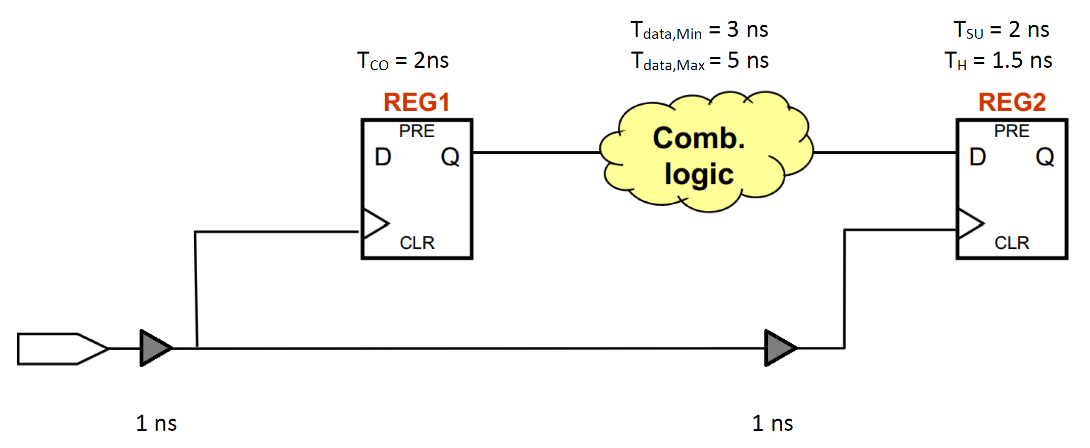
Problem 1
Calculate the setup and hold slack if the clock runs at 150 MHz. Does the system meet timing requirements? Make sure your submitted PDF includes your work.
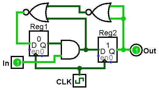
Problem 2
|
|
Solve for the setup slack and hold slack for this circuit. Make sure your submitted PDF includes your work.
Problem 3
A 2-D rotation of the point (x,y) by θ radians is a very common operation in computer graphics and results in the point (,), where =x·cosθ-y·sinθ and =x·sinθ+y·cosθ. Glossing over the exact number representation and bit manipulation, a circuit that computes this rotation can be represented as shown below.
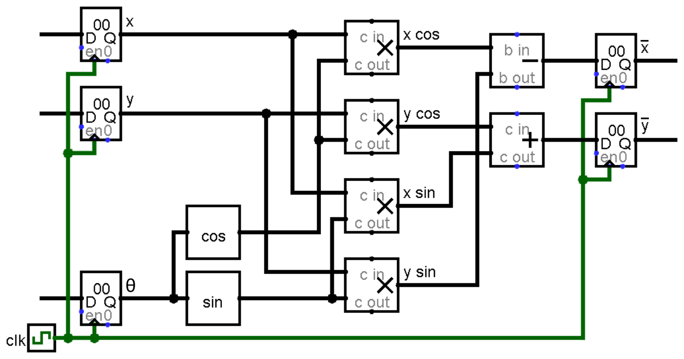
For simplicity, assume that tsu = th = twire = tclk = 0 and that tCO = 10 ns for all registers. The logic delays are as follows:
- tcos = 100 ns, tsin = 90 ns
- tmult = 60 ns
- tadd = 25 ns, tsub = 30 ns
- Construct a Data Flow Graph (DFG) for the circuit. Label your three starting inputs x, y, and θ for each of the respective registers, and your outputs and .
- Draw two cut sets on your DFG, one that makes a 2-stage pipelined and one that makes a 3-stage pipelined version of the circuit. Your pipelined circuits should have the minimum possible clock periods. You should use two copies of your DFG or make sure that the different cut sets are clearly distinguishable on a single DFG.
- Assuming we use the minimum clock periods, compute the latency for both your 2-stage and 3-stage pipelined versions of the circuit.
Problem 4
This part of the homework is an exercise create by Intel for using the Quartus Prime Timing Analyzer. You will need to download TimingAnalyzer.qar (files).
Part 1: Project Setup in Quartus Prime Lite
- Double-click to open TimingAnalyzer.qar. If you see a message about Max10, you have the wrong TimingAnalyzer.qar file!
- A dialogue box will appear.
Select a destination folder or use the default location and press
OK.
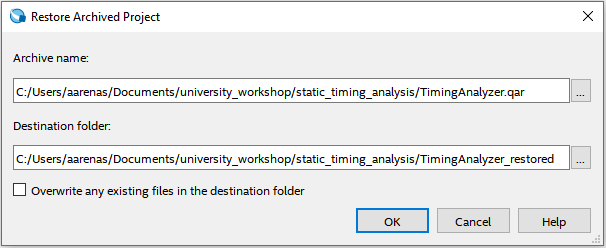
Figure 4: Dialogue box that restores the .qar file. - In the Project Navigator, click Hierarchy
and select Files from the drop-down menu.
Double-click on TimingAnalyzer.v to view the Verilog file.
It adds two 128-bit numbers and then multiplies the sum by a 32-bit
number.
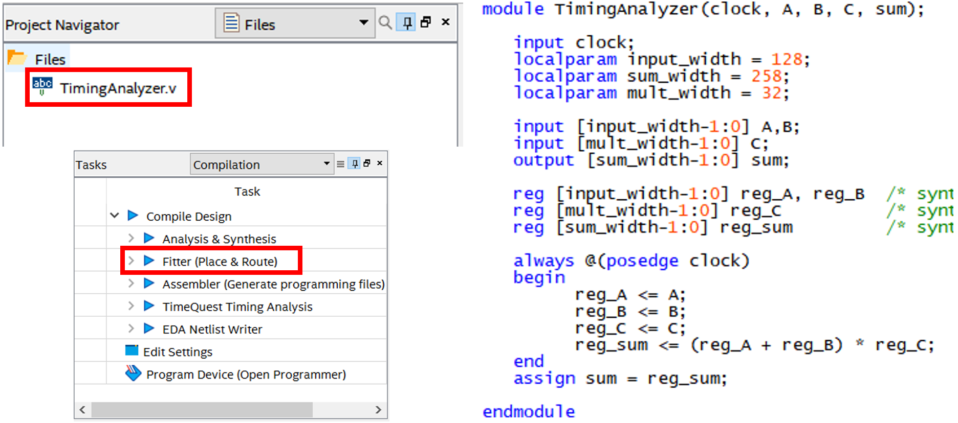
Figure 5: In the Project Navigator (top-left), clicking the highlighted title will open the Verilog file (right) for Step 3. The Tasks pane in Quartus (bottom-left) is needed for Step 4. - Perform an initial compilation by either double-clicking "Fitter (Place and Route)" in the Tasks pane or by going to Processing → Start → "Start Fitter". Before applying timing constraints, we need to create an initial database generated from the post-map results of the design. This can also be done with post-fit results, which requires a full compilation.
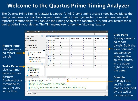
- Select Tools → "TimeQuest Timing Analyzer" or click the blue clock icon.
Part 2: Using the Quartus Prime Timing Analyzer
- The first thing to do when Timing Analyzer is open is to create a
timing netlist.
This is done by double clicking "Create Timing Netlist" in
the Tasks pane.
This cannot be done before the initial compilation; Create Timing
Netlist requires a post-fit or post-map database.
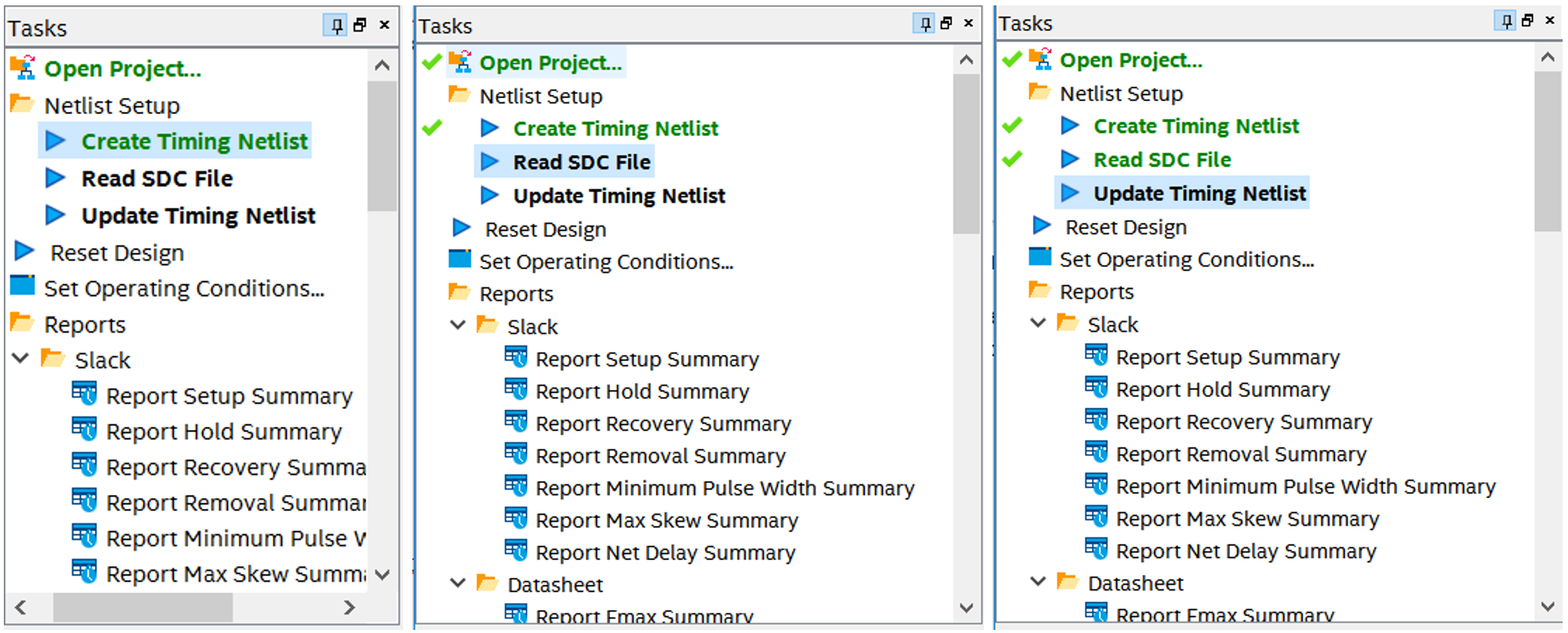
Figure 7: (Left – Step 6) The Tasks pane in Timing Analyzer. Double-clicking any of the blue play buttons will execute the action.
(Middle – Step 7) Double-clicking "Read SDC File" will read in the created constraints.
(Right – Step 8) Double-click "Update Timing Netlist" to access all the reports available. - For now, there is no Synopsys Design Constraints (SDC) file in our project. Timing Analyzer will create a default SDC file with one clock when none is found. Double-click "Read SDC File" to generate and read this SDC. In the rest of this exercise, you will overwrite this SDC file with your own constraints created in Timing Analyzer.
- Update the timing netlist by double-clicking
"Update Timing Netlist".
This creates summaries and reports with useful information.
To save time, you can double-click "Update Timing Netlist" without doing Steps 6 and 7 individually. Doing this automatically runs the "Create Timing Netlist" and "Read SDC File" commands.
- First, create a clock for the design.
Do this by going to the main menu and clicking Constraints →
"Create Clock…".
- Name it clock and give it a period of 12.5 nanoseconds.
- Set rising time to 0 and falling time to 6.25 nanoseconds (50% duty cycle).
- For the targets section, click "…" to
search for the clock or just type in exactly what you see in
the figure below.
- If you clicked "…" then the Name Finder from Figure 5b will open. Press List in the dialogue box that appears. Scroll down to select clock. Either double-click it or highlight it and press > to add your selection. Finally, press OK. Your Create Clock window should be identical to the one below. You may click "list" and don't find the "clock" in the list but if you write what you see exactly in the "create clock" pane it should be fine.
When the Create Clock window is identical to the one below, press Run.
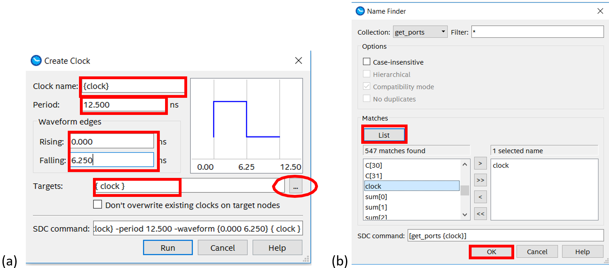
Figure 8: (a) The Create Clock dialogue window. Click on the "…" at the end of the targets section to open the Name Finder window to specify the clock. (b) The Name Finder window where you select your targets for the Create Clock command. When you change a design constraint, the background page will be yellow and show "OUT OF DATE" until you update the page again. - On the Tasks pane, scroll down to Diagnostics
and double-click "Report Clocks" to see what clocks are
driving this system.
Doing this updates Timing Analyzer with the most recent
constraints, so the "OUT OF DATE" yellow page will go away.
Here we find the clock that we just created:
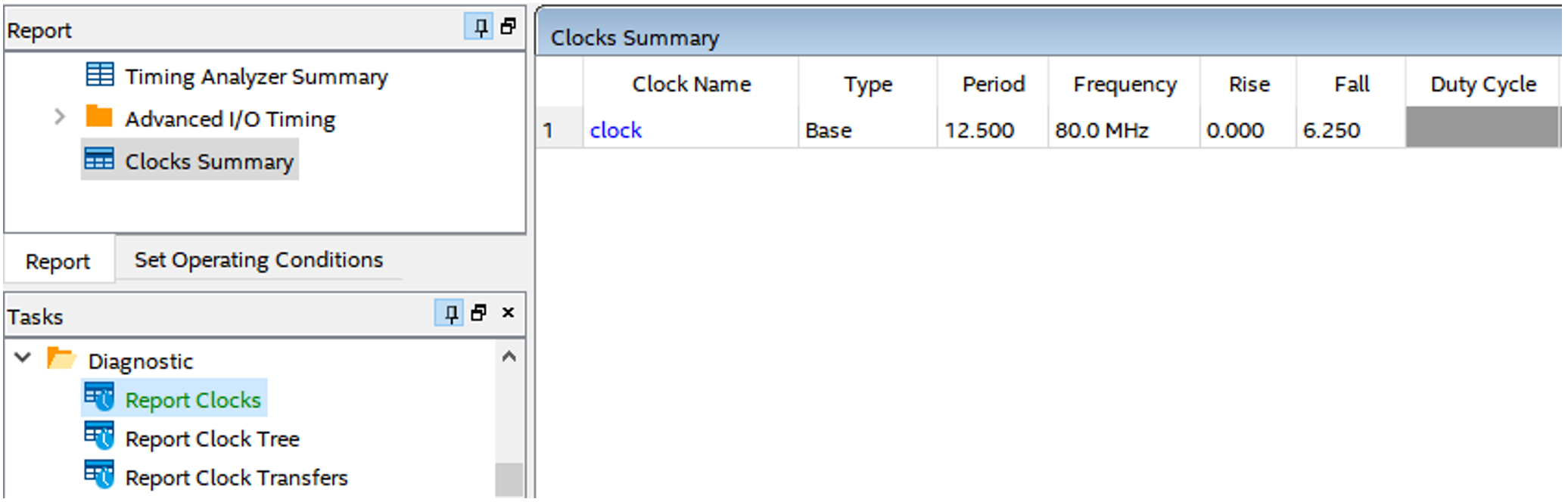
Figure 9: The clocks in the system followed by all the attributes of the clock. - To access any of the reports, find those of
interest in the Tasks pane and double-click them.
The next steps will look into "Report Setup Summary" and
"Report Hold Summary" to check if our synchronous adder
meets setup and hold requirements.
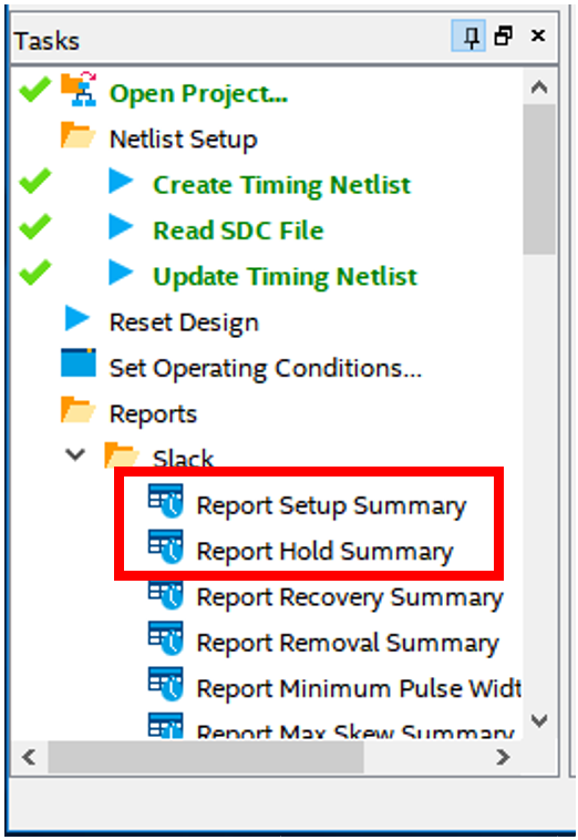
Figure 10: Double-click a report in the Tasks pane to open it. - Double-clicking "Report Setup Summary"
shows us the setup slack of our design.
If it is red and negative, then it fails the timing requirements.
If it is black and positive, then it passes the timing requirements.
- The "End Point TNS" column in the report reports the total negative slack, the negative slack of all possible paths summed together.
- The "Slack" column reports the slack of the data path that fails the worst.
- The "Clock" column reports which clock drives the design.
Your results may vary from the following screenshots:
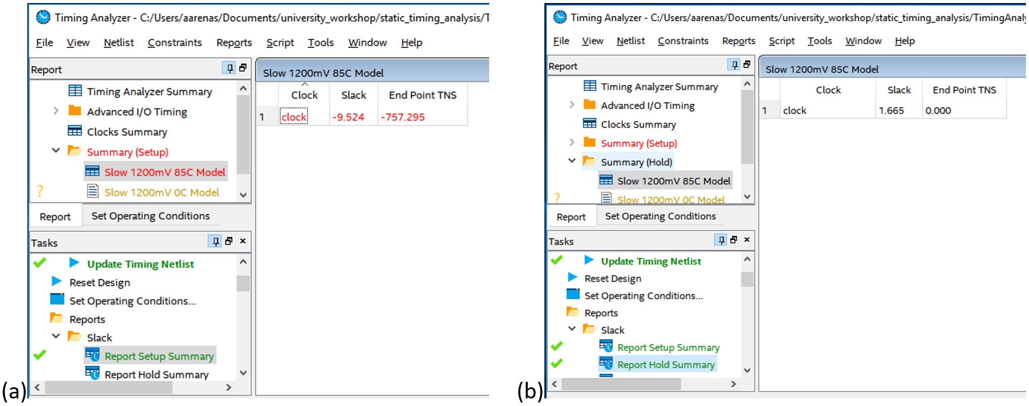
Figure 11: (a) The setup slack of our design. It is red and negative, meaning that the setup slack requirements were not met. (b) The hold slack of our design. It is black and positive, meaning that the hold slack requirements were met. - Double-clicking "Report Hold Summary" reveals that hold timing passes. Here, the path that comes closest to failing timing has 1.665 ns of slack. Your results may vary from the above screenshot.
- Generate a timing report on our clock to
investigate the setup violation.
Do this from the Report Clocks summary window.
- Open the dialogue box shown to the right by
either:
- Right-clicking clock and then clicking "Report Timing…" OR
- Scrolling down in the Tasks pane to "Custom Reports" and double-clicking "Report Timing…".
- The Clocks section allows you to decide which clock in the design you want the report on. There is only one, so select clock as shown in Figure 12.
- The "Analysis Type" section determines which report you will see. Select Setup first.
- The Paths section allows us to select how many paths will be shown. It will show the paths that have the least slack first, so entering 1 will show us the single worst path.
- Finally, click "Report Timing" to see this custom report.
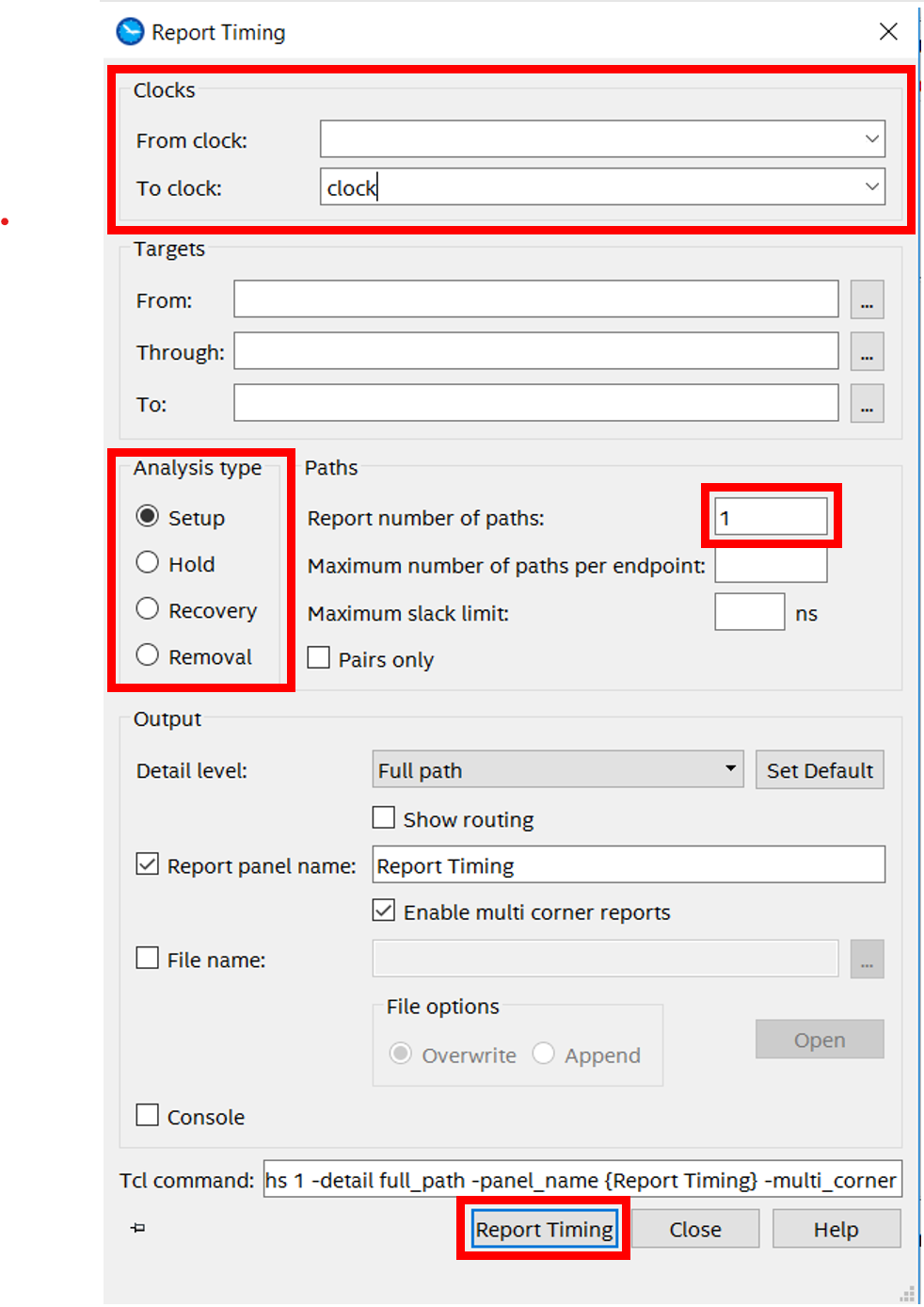
Figure 12: The "Report Timing…" dialogue box. - Open the dialogue box shown to the right by
either:
- The resulting report has several parts of interest:
- Under "Summary of Paths" (tab in the top window), the first column shows the setup slack of the paths that fail timing the worst in descending order. The next two columns define where this path starts and ends, followed by other clock details.
- The "Data Arrival Path" (in the "Data Path" tab in the lower-left window) is equivalent to the Data Arrival Time from the slack equation, but shown in much more detail. It is possible to trace the entire path with the information shown below.
- The "Data Required Path" is similarly equivalent to the Data Required Time from the slack equation. These values can be used to manually confirm Timing Analyzer's result for setup slack.
- The Waveform viewer on the bottom-right gives a graphical view of each of the components in the slack equations.
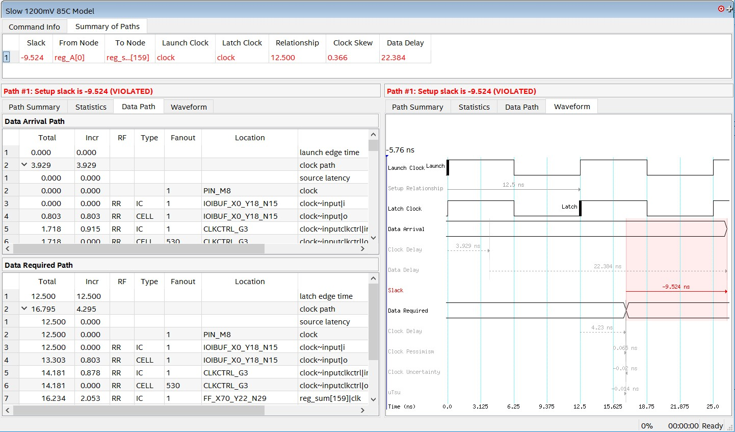
Figure 13: The result of the custom timing report. - Setup Slack = Data Required Time – Data
Arrival Time.
First, trace the "Data Required Path" to find all the delays
along the clock path to the destination register.
- The Total column counts all of the delay up to that point.
- The Incr column shows the increment by which each row adds to the delay.
- The Type column describes where the delay originates from.
- The Fanout column shows how many outputs leave that unit.
- The Location column tells you where in the FPGA it can be found.
- The Element column describes what part of the design we are describing.
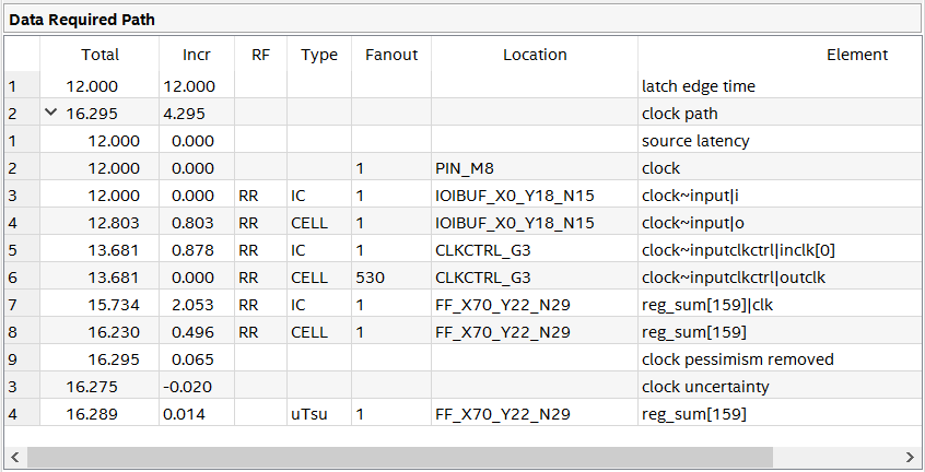
Figure 14: The "Data Required Path," whose total delays add up to equal the data required time. - Trace the "Data Arrival Path" to view all
the delays involved in the data's transfer from the source to the
destination register.
Use the Location column to see where in the FPGA the data is.
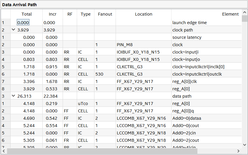
Figure 15: The "Data Arrival Path," whose total delays add up to equal the data arrival time. - What element adds the most delay? How can we change the clock parameters such that setup slack does meet timing requirements?
- Repeat the "Report Timing…" steps to investigate the hold slack results. Does the same element add the most delay for hold slack? Why does this make sense?
- Edit the clock constraint such that setup slack no
longer fails timing.
This can be done directly in the SDC file or by using the Timing
Analyzer GUI:
- Double-click on "Report Clocks" in the Tasks pane.
- Right-click clock and select "Edit Clock Constraint…".
- Enter the clock period that would make setup slack pass timing requirements. Make sure the rising time is at 0 and the falling time is at half of the clock period.
- Once finished, hit Run.
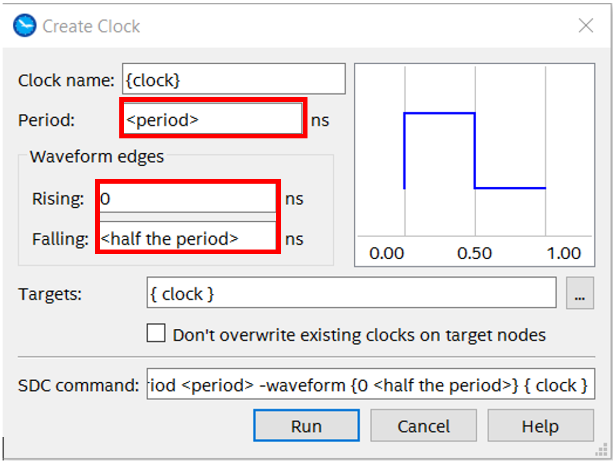
Figure 16: The "Create Clock" GUI in Timing Analyzer allows you to specify clock frequency, as well as rising and falling times. It presents the equivalent SDC command in the bottom text box. Edit the highlighted boxes to make setup slack meet timing requirements! - The "Clocks Summary" window should now be
yellow and show that it is out of date.
Write the recent clock creation to an SDC file by selecting
Constraints → "Write SDC File…" and the newly created
clock will overwrite the default one in the SDC file.
Your dialogue box should look exactly the same as Figure 17.
Press Ok.
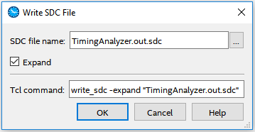
Figure 17: The "Write SDC File…" dialogue box for saving an SDC constraint created in the GUI. - Double-click "Update Timing Netlist" to
view the new reports from your design with the updated clock.
You can see the updated clock in the "Report Clock" summary
page now.
Double-click on "Report Setup Summary" to see if timing is
met with these new conditions.
Your results will differ from the following screenshots depending
on your chosen clock period.
What is the fastest frequency you can set the
clock to for this to pass setup timing?
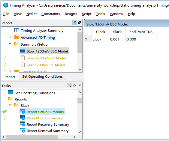
Figure 18: The new setup summary reveals that timing does pass if the clock is adjusted to the proper frequency. - Generate another timing report exactly as you did in Step 14 by selecting "Custom Reports" → "Report Timing…" in the Tasks pane. The design now passes timing. Investigate how it's different.
- Timing Analyzer only works completely when the
designer enters constraints for all possible paths and clocks.
Check if there are unconstrained paths by scrolling down in the
Tasks pane in the Diagnostics section and double-clicking
"Report Unconstrained Paths."
A completely constrained design has 0 unconstrained ports, paths,
and clocks.
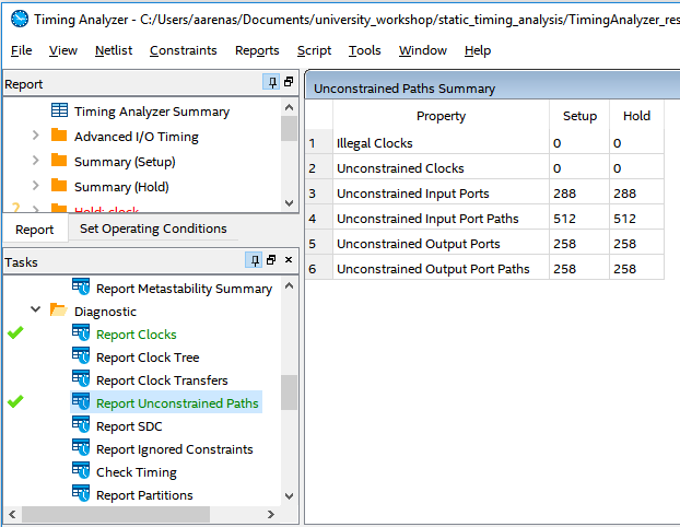
Figure 19: The report containing the number of unconstrained paths in the design. - Constrain the input ports and paths by adding a
minimum and maximum set_input_delay.
- To add the constraints in Timing Analyzer, click Constraints → "Set Input Delay…". Use -0.5 ns as the minimum delay and 6.5 ns as the maximum delay (i.e., do steps 25 & 26 for each).
- After setting the clock name to clock and the delay value to the proper number, click the "…" to the right of the Targets section highlighted below to add all the inputs.
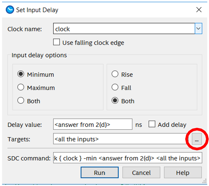
Figure 20: The set_input_delay GUI window. - Press List to see all the ports in our
design.
Select every port that begins with A, B, and C (besides
clock) and press the > button to add
them.
Press OK.
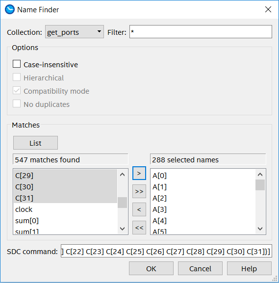
Figure 21: The window that selects which ports to apply the set_input_delay to. - The Unconstrained Paths Summary should now have a yellow background with "OUT OF DATE" watermarks across the page. Double-click "Report Unconstrained Paths" in the Tasks pane to update it with your recent actions. Set the min output delay to -0.5 ns and max output delay to 5.6 ns for all sum outputs. Double-clicking "Report Unconstrained Paths" from the Tasks pane should reveal that there are zero unconstrained paths remaining.
- Once you've finished adding all the constraints, click Constraints → "Write SDC File…" to save them (same as Step 21 and Figure 17). Now open the SDC file from your working directory. Look around and see how much time Timing Analyzer saved you by making all these for you! There should be the created clock, as well as all the minimum and maximum set_input_delay and set_output_delay constraints you created.
- All the new constraints, however, have created a
hold violation within our system.
Double-click "Report Hold Summary" to verify this.
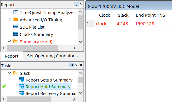
Figure 22: The hold slack report that reveals the hold violation. - To fix the hold violation, we will first add our
SDC file to the Quartus project and then re-run the fitter.
It will take into account every constraint we have made when making
decisions for how to route the design.
To add the SDC file, go back to the Quartus window and click
Project → "Add/Remove Files in Project…".
- Click "…" and navigate to your working
directory.
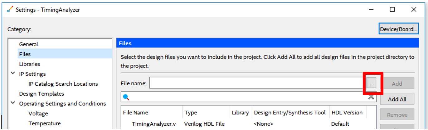
Figure 23: The "Add/Remove Files in Project…" dialogue window. - Change the file type to "All Files (*.*)".
Find the .sdc file and select it.
Press Open.
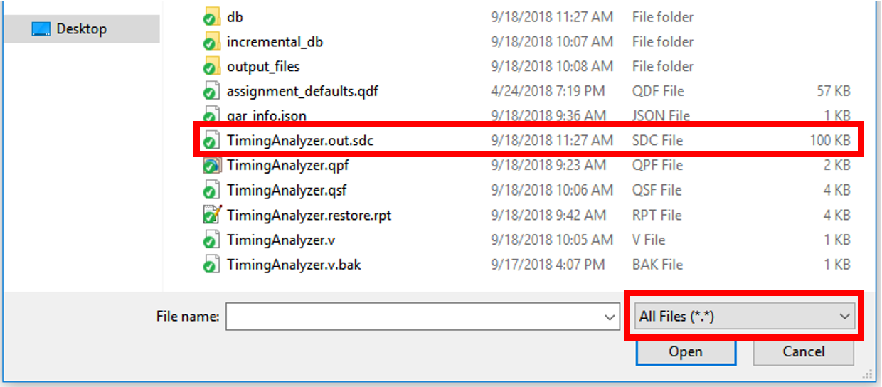
Figure 24: To select the .sdc file, change the file type to "All Files" and select the only SDC file you see. - Press Ok.
You have now added the SDC file to your design.
Verify it is there by going to your Project Navigator and
selecting Files from the drop-down tab.
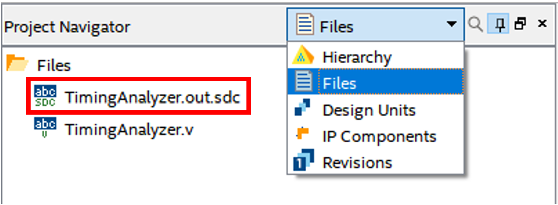
Figure 25: The Project Navigator showing the list of files in the project. - Finally, run the Fitter again. This time the Fitter will make decisions while considering all the user entered timing constraints.
- Click "…" and navigate to your working
directory.
- Open Timing Analyzer again. In the Tasks pane, double-click "Update Timing Netlist" and then double-click "Report Hold Summary." The design should now pass both setup and hold timing requirements!
- Temperature and voltage have known effects on the
speed of a circuit.
Quartus by default will assume "Slow 1100mV 85C Model" (the 1200 mV
shown in the image below is for another board).
We can change this using the "Set Operating Conditions" tab.
You will see additional options (Slow/Fast, 85C/0C).
Select each new model and then double-click "Report Setup
Summary" in the Tasks pane to compute the setup slack for that
model.
The corresponding model name under the "Summary (Setup)" folder in
the Report pane will change from yellow to black or red.
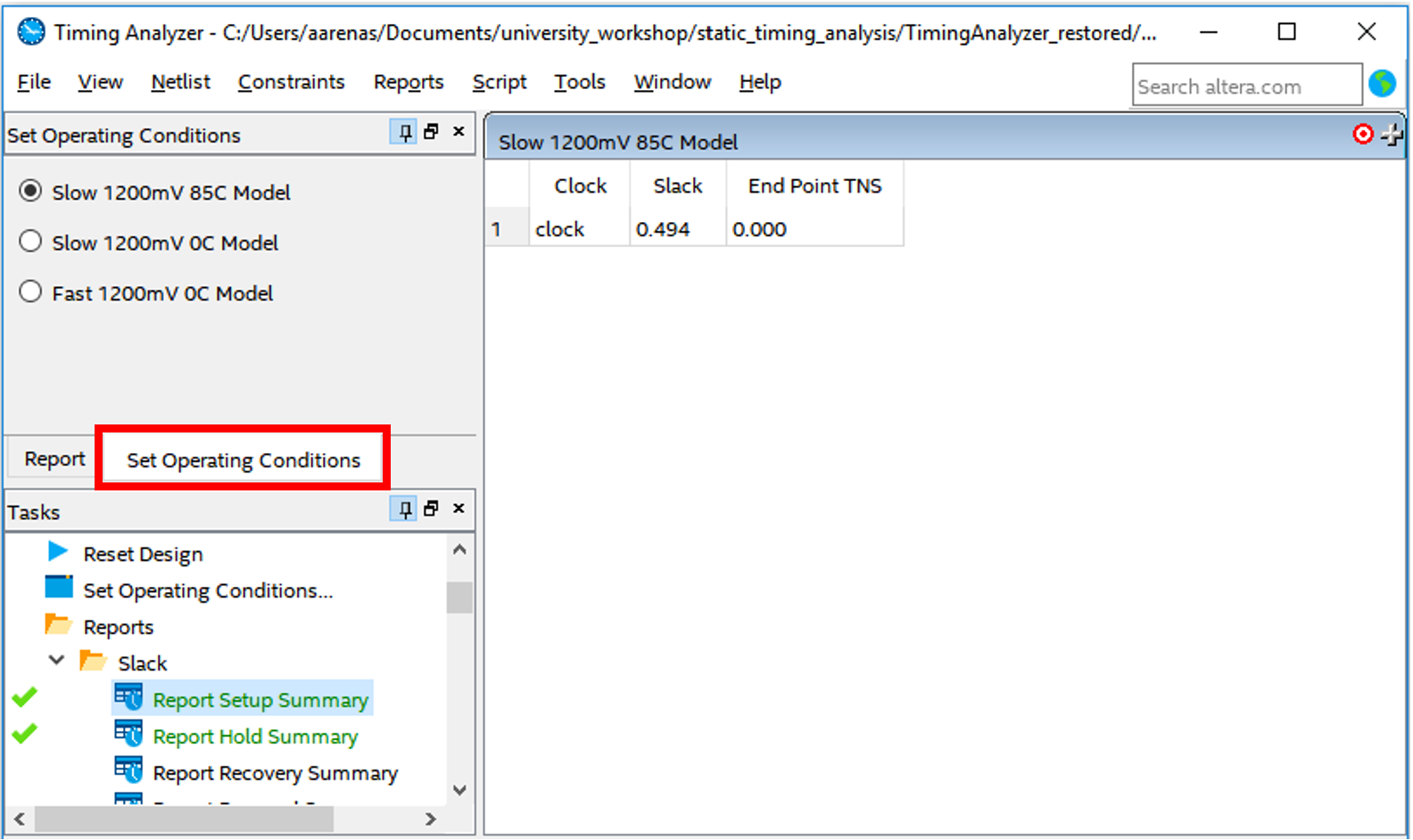
Figure 26: Clicking Set Operating Conditions will allow the designer to choose from one of three conditions Quartus makes timing calculations based off of. The numbers will vary depending on the frequency/period you selected for your clock. - Now use the "Summary (Setup)" reports to answer
the following questions:
- Which of the options has the most setup slack?
- How does increasing voltage speed change the speed of a circuit?
- How does increasing temperature change the speed of a circuit?
- Repeat Steps 32-33 for hold slack.
Grading Rubric
- Setup and hold slack
- Setup and hold slack
- 2- and 3-stage cutsets and latency calculations
- Responses for Step 18 (x2)
- Responses for Step 19 (x2)
- Response for Step 22
- Responses for Step 33 (x3) for setup slack
- Responses for Step 33 (x3) for hold slack