HW 3: Buffers and ASM
Problems
Problem 1
You are provided (files) with three SystemVerilog files that implement the FIFO buffer shown below (fifo.sv, fifo_ctrl.sv, reg_file.sv) and an empty test bench (fifo_tb.sv).
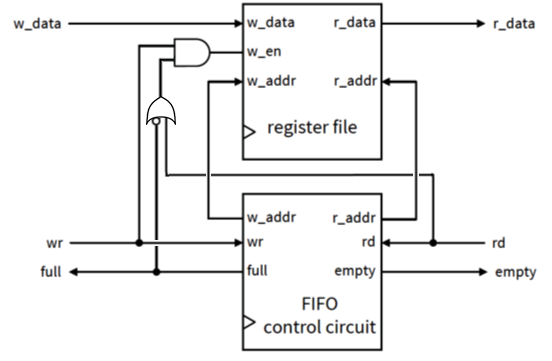
In some applications, the widths of the write port and read port of a FIFO buffer are not the same. For example, a subsystem may write 16-bit data into the FIFO buffer and another subsystem only reads and removes 8-bits of data at a time.
Assume that the width of the write port is twice the width of the read port. Once written, the upper half (i.e., most significant bits) of the data should be read before the lower half.
- Redesign the FIFO with a modified controller and register file
and verify its operation.
The
DATA_WIDTHparameter should be the width of the read port. - Briefly explain your approach: describe at a high level the changes you made to the code and how you verified that it works correctly. Be sure to provide your simulation results.
Problem 2
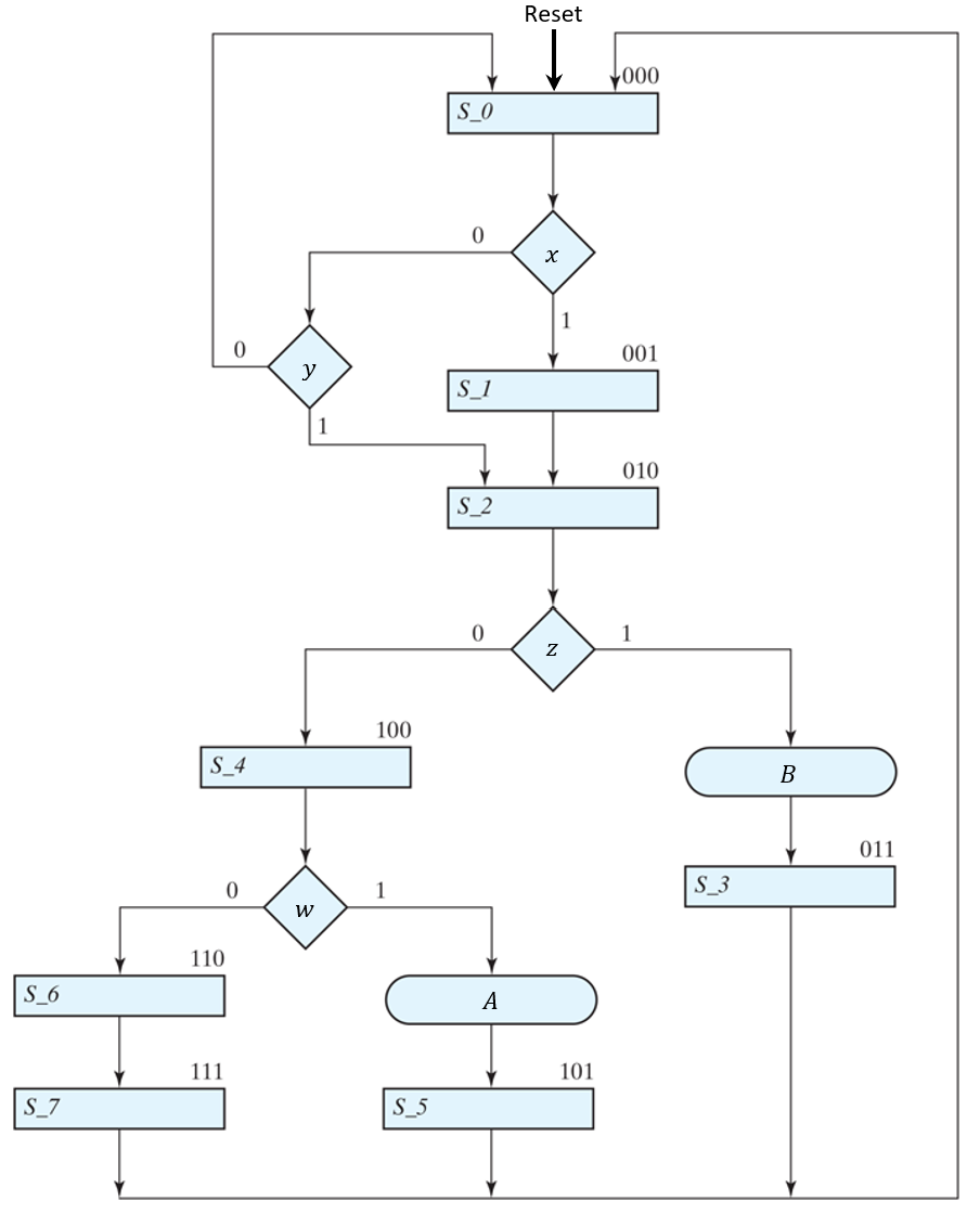
An ASM chart is shown below.
- Draw the equivalent state diagram. You do not need to include the states' binary encodings on your diagram.
Problem 3
The ASM chart for Example #4 from Lecture 5 is reproduced below.
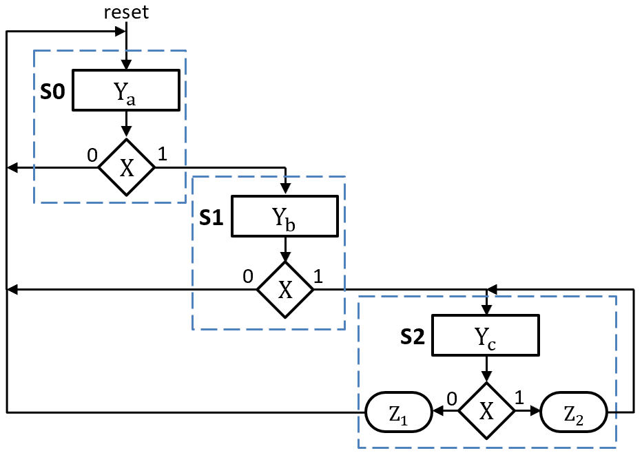
- Implement the ASM chart and a thorough test bench in the provided
files hw3p3.sv and hw3p3_tb.sv
(files).
- Do NOT modify the given port names, including both spelling and capitalization.
- Make sure to use both
psandnsas state signals. - You should simulate the test bench to verify the expected behavior, but do not need to submit a screenshot or explanation of the simulation.
- Describe/explain the difference in timing between the Moore and Mealy outputs. How do the ASM blocks help indicate the timings?
- In your opinion, how does tracing an ASM chart compare to tracing an FSM diagram?
Submission Requirements
Due by the end of the deadline day, submit your solutions (e.g., text, diagrams, screenshots, work) as a single PDF file ending in .pdf (all lowercase) to .
- Include the requirements listed in the .
- At the end of your document, estimate how long you
spent working on the homework and rate the difficulty on the
following scale:
Very Hard — Hard — Moderate — Easy — Very Easy - As separate files, upload your commented
SystemVerilog files (.sv), including test benches.
- fifo.sv
- reg_file.sv
- fifo_ctrl.sv
- fifo_tb.sv
- hw3p3.sv
- hw3p3_tb.sv
Grading Rubric
- Modified buffer should work in "normal" situations as well edge cases (e.g., empty, full)
- Applicable situations should be shown and pointed out in simulation
- Design decisions should be explained
- Implementation and simulation (autograded)
- Three responses: a description/explanation, a question response, and an opinion