HW 2: Memories
Problems
Problem 1
Specify the minimum size (i.e., number of words and number of bits per word) of separate ROMs that will accommodate the truth tables for the following combinational circuit components. Assume the output will be as wide as is needed to represent the largest possible result (no truncation).
- A binary multiplier that multiplies two 4-bit binary words.
- A 3-bit adder-subtractor.
Problem 2
The following questions may depend on each other and are intended to be done in order:
- How many 4 Mi × 16 RAM chips are needed to provide a total memory capacity of 64 Mi-bytes?
- How many address bits are needed for our larger, 64 Mi-byte-memory assuming the same word size as the individual chips?
- How many of the address bits are connected to each RAM chip?
- How many of the address bits must be decoded for the chip select (i.e., how many are needed for us to know which RAM chip we need to access)? Specify the size of the decoder.
Problem 3
You are given (files) two different implementations of a 4-bit sign-and-magnitude adder: (1) a SystemVerilog module found in sign_mag_add.sv and (2) a corresponding ROM table found in truthtable4.txt.
- Complete the testbench in sign_mag_add_tb.sv for an
instance of sign_mag_add named dut1 with
output signal sum.
Make sure that you include different test cases that cover at least
the following situations:
- Some number + 0
- pos + neg = 0
- pos + neg > 0
- pos + neg < 0
- pos + pos (valid)
- pos + pos (overflow)
- neg + neg (valid)
- neg + neg (overflow)
- Modify the following code (provided for you in
sync_rom.sv) to instead work with the data found in
truthtable4.txt (which you should open to view).
If you open truthtable4.txt in Quartus, don't add
the file to your project.
module sync_rom (input  logic clk,
                 input  logic [3:0] addr,
                 output logic [6:0] data);
   // signal declaration
   logic [6:0] rom [0:15];
   // load binary values from a dummy text file into ROM
   initial
      $readmemb("data.txt", rom);
   // synchronously reads out data from requested addr
   always_ff @(posedge clk)
      data <= rom[addr];
endmodule  // sync_rom
The $readmemb argument shown ("data.txt") uses a relative path. If you encounter the following warning in ModelSim (memory will also show up as all X's and a red line):"# ** Warning: (vsim-7) Failed to open readmem file "data.txt" in read mode."
Solution: Replace the argument with the absolute path (e.g.,"C:/371/hw2/data.txt"). - Add an instance of sync_rom named
dut2 with output signal data in your
testbench from Part A alongside dut1 and verify that they
produce the same behavior in ModelSim when passed the same
inputs simultaneously.
- Depending on when you change the inputs in your test bench, you should see a timing difference of 0-1 clock cycle between the outputs of the two.
- Submit your modified code files, but you do not need to include a screenshot of your simulation in your submission PDF.
- Compare the resource usage of these two implementations. Synthesize in Quartus with sync_rom.sv and then sign_mag_add.sv as your top-level module. Find the "Resource Usage Summary" page in the Compilation Report and compare the number of ALMs and memory bits used (omission means 0). Include this comparison in your submission PDF.
Problem 4
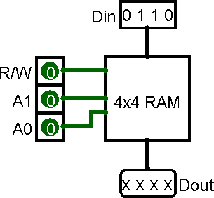
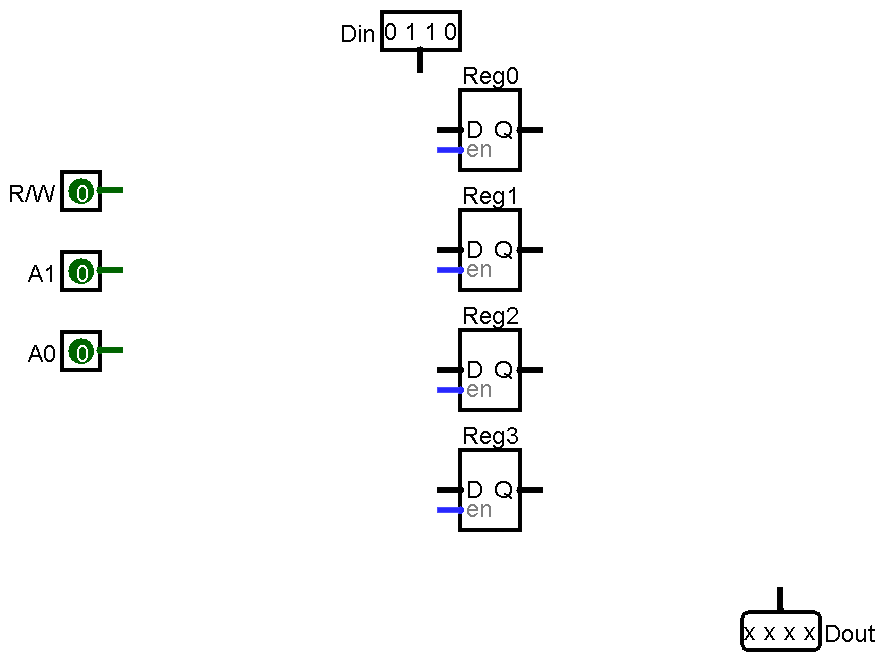
Let's examine a 4×4 RAM module as shown below.
- The R/W input is 1 for writing and 0 for reading.
- A1A0 forms the two-bit address that selects which word is read out to Dout.
In the following parts, draw out a memory diagram by adding/using wires, gates, and plexors (i.e., multiplexors or demultiplexors). The clock inputs are not shown, but should be assumed to be present and connected correctly.
- Complete the diagram below for an implementation of the 4×4 RAM
as a register file.
The en inputs to the registers are enable signals
(i.e., the register will update when en=1 and
remain the same when en=0).
- Construct an 8×8 memory diagram using the given 4×4 RAM as a building block. Hint: how will the inputs and outputs differ for a 8×8 RAM compared to the 4×4 RAM block diagram shown above?
Submission Requirements
Due by the end of the deadline day, submit your solutions (e.g., text, diagrams, screenshots, work) as a single PDF file ending in .pdf (all lowercase) to .
- Include the requirements listed in the .
- At the end of your document, estimate how long you
spent working on the homework and rate the difficulty on the
following scale:
Very Hard — Hard — Moderate — Easy — Very Easy - As separate files, upload your commented
SystemVerilog files (.sv), including test benches.
- sign_mag_add.sv
- sign_mag_add_tb.sv
- sync_rom.sv
Grading Rubric
- Answer the 2 questions
- Answer the 4 questions
- Implementations and simulations
- Memory usage comparison
- Two circuit diagrams