Here we will be discussing how to create a heirarchical design using a combination of ABEL and schematic. To do this, we take the example of the shift register which we did earlier using only ABEL. Now we implement the universal shift register using a combination of ABEL and schematic.
Our goal is to design a 4-bit universal shift register. It should implement the following functions specified by it's S2, S1, S0 control inputs: (000) Hold, (001) Circular Right Shift, (010) Circular Shift Left, (011) Logic Shift Right, (100) Logic Shift Left, (101) Arithmetic Shift Right, (110) Arithmetic Shift Left, (111) Parallel Load. Your shift register sub-module should consist of a cell with a single flip-flop and three inputs(DI, SR, and SL). There should also be two control inputs: S0 and S1. When S0 and S1 are (11), DI should be loaded into the flip-flop, for (01) SL should be loaded in, for (10) SR should be loaded in, and for (00) the flip-flop should hold it's current state.
We will implement the design by writing three ABEL modules mux41, shdec, shift and a top-level schematic shiftreg.
shift
This ABEL module represents a D flip-flop with inputs D and a clk and ouput Z. It simply loads the input D to the output Z at the positive edge of the clock clk.
mux41
This a 4:1 multiplexer with data inputs DI, SL, SR and OH and control inputs S0, S1 and output OUT. When S0 and S1 are (11), DI is loaded into the flip-flop through the OUT output of the mux, when they are (01) SL is loaded in, for (10) SR is loaded in, for (00) the flip-flop holds it's current state i.e. the input of the flip-flop equals its output.
shdec
This module performs the Hold, Circular Right Shift, Circular Shift Left, Logic Shift Right, Logic Shift Left, Arithmetic Shift Right, Arithmetic Shift Left and Parallel Load when the control inputs S2, S1, S0 are 000, 001, 010, 011, 100, 101, 110 and 111 respectively. To do this, the schematic shdec has inputs S0, S1, S2 and E and outputs CR, CL, AR, OUT0, OUT1. The OUT0 and OUT1 outputs control the S0 and S1 inputs of the module mux41 and the CRand AR outputs of this module controls the SR input of module mux41 and the output CL is used to control the input SL.
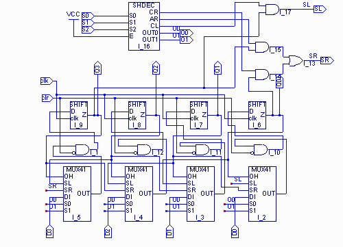
shiftreg
This is the top-level schematic that manages the three modules explained above to implement the 4-bit universal shift register. This schematic creates one copy of module shdec four copies of the modules mux41 and shift. The output OUT of mux41 provides the input to the flip-flop in the module shift and the inputs of mux41 are in turn controlled by the outputs of shdec and the inputs D0, D1, D2, D3 of the schematic shiftreg. The ouputs of this top-level schematic Q3..Q0 are the outputs of the 4-bit universal shift register.
MODULE shift

        interface(D,clk -> Z);

TITLE 'shift register'

"Inputs
   D,clk        pin;

"Outputs
   Z            pin istype 'reg, buffer';

EQUATIONS

   Z.clk = clk;
   Z := D;

END
MODULE mux41

        interface (OH,SL,SR,DI,S0,S1 -> OUT);

TITLE '4 : 1 multiplexer'

"Inputs
   OH,SL,SR,DI,S0,S1            pin;

"Outputs
   OUT                          pin istype 'com';


EQUATIONS

        OUT = (!S0 & !S1 & OH)
              # (!S0 & S1 & SL)
               # (S0 & !S1 & SR)
                # (S0 & S1 & DI);


END
MODULE shdec

        interface(S0,S1,S2,E -> CR,CL,AR,OUT0,OUT1);

TITLE 'decoder for shift operations'
"Inputs
  S0,S1,S2,E            pin;

"Outputs
  CR,CL,AR,OUT0,OUT1    pin istype 'com';

"Aliases
  S = [S2,S1,S0];
  OUT = [OUT1,OUT0];

EQUATIONS

        CR = (E & !S2 & !S1 & S0);
        CL = (E & !S2 & S1 & !S0);
        AR = (E & S2 & !S1 & S0);
        WHEN (S == 0) THEN
                OUT = 0;
        ELSE WHEN (S == 1) THEN
                OUT = 1;
        ELSE WHEN (S == 2) THEN
                OUT = 2;
        ELSE WHEN (S == 3) THEN
                OUT = 1;
        ELSE WHEN (S == 4) THEN
                OUT = 2;
        ELSE WHEN (S == 5) THEN
                OUT = 1;
        ELSE WHEN (S == 6) THEN
                OUT = 2;
        ELSE WHEN (S == 7) THEN
                OUT = 3;

END