CSE370 Catalog of Parts in the Laboratory Design Kit
There is one of each of these parts in the kit except where noted. The chips are designed to straddle the trough in the breadboard with two rows of pins. One row is lined up on one side of the trough on column "e" and the other row lines up with column "f" on the other side of the trough. Don’t insert the chips with both rows of pins on one side of the trough as this will connect corresponding pins across the chip and will lead to non-functional designs and quite possibly damage the parts. All the chips have their catalog part number stamped on their top (when oriented so that you can read it, pin #1 will be on the bottom left and the numbering will proceed counter-clockwise from there) in the form SN74HCTXXN where the XX will be a two or three digit number that will differ on each chip. This specifies the function of the chip, the rest of the code specifies the implementation technology. The index below uses the number XX to define the pins of each chip. The ground pin is usually labeled GND and is the rightmost pin on the bottom row, the power pin is usually labeled VCC or VDD and is the leftmost pin on the top row.
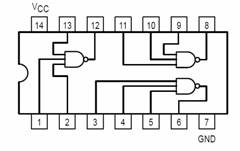
’00 – 4 2-input
NAND gates:
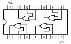
’02 – 4 2-input
NOR gates:
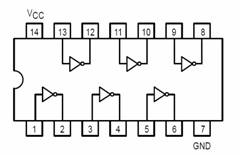
’04 – 6 inverters
(2 of these in the kit):
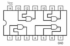
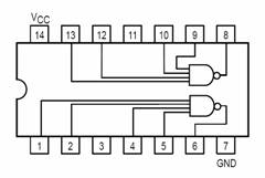
’10 – 3 3-input
NAND gates:
’14 – 6 inverters
with Schmitt trigger:
’20 – 2 4-input
NAND gates:
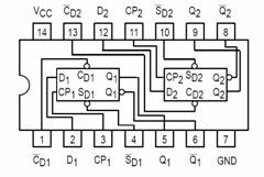
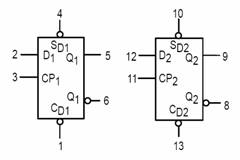
’74 – 2 D-FFs with set and clear inputs:
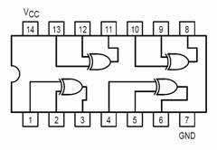
’86 – 4 XOR gates:
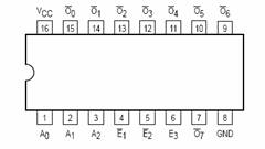
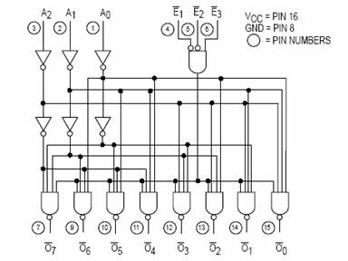
’138 – 3:8 decoder with 3 enables:
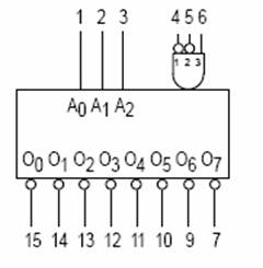
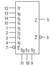
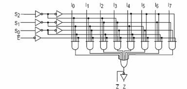
’151 – 8:1
multiplexer with enable and complementary outputs:
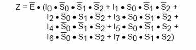
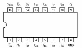
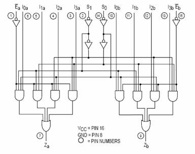
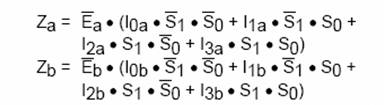
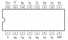
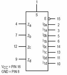
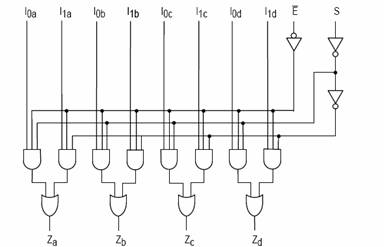
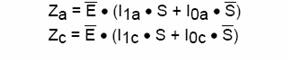
’153 – 2 4:1
multiplexers with common select and separate enable:
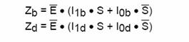
’157 – 4 2:1
multiplexers with common select and enable:
’244 – 8 tri-state
buffers with common enable:
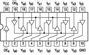
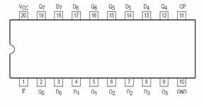
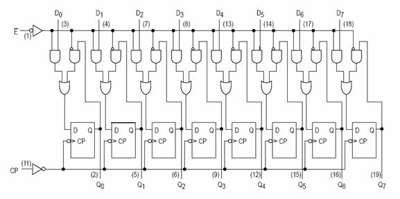
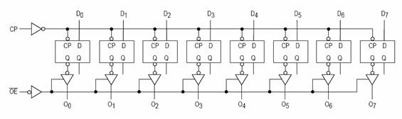
’374 – 8 D-FFs with common output enable:
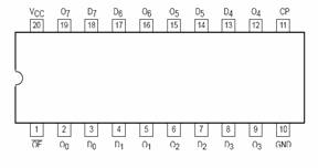
’377 – 8 D-FFs with input enable: