CSE 370 Laboratory Assignment
Applying Your Knowledge
Assigned: Monday, May 31, 2010
Due For Full Credit: 6:30PM, Friday, June 4, 2010 **Note, check-offs will be given at <TBD> times until
Wednesday June 9th, for partial credit.**
Objectives
The objective of this lab is to complete the LCD/Magnetic
Stripe Card-Reader lab. Now that you have built the LCD control logic and wired
it up so that switches drive which character the LCD writes; it is time to
change that so that the magnetic stripe reader drives which character the LCD
writes. Lab 9 should be easier than Lab 8 because you have already laid the
foundation for proper timing.
Before You Begin
There are several datasheets involved in this lab. One of
them is the Magnetic Card Reader
Specifications. This specification is mostly correct; however the pin-outs
indicated on the specifications are NOT THE ONES YOU
WILL BE USING. Use the pin-outs described to you in this lab write-up,
or else you will have wiring problems and your magnetic card reader will not
interface correctly with code and LCD.
Tasks:
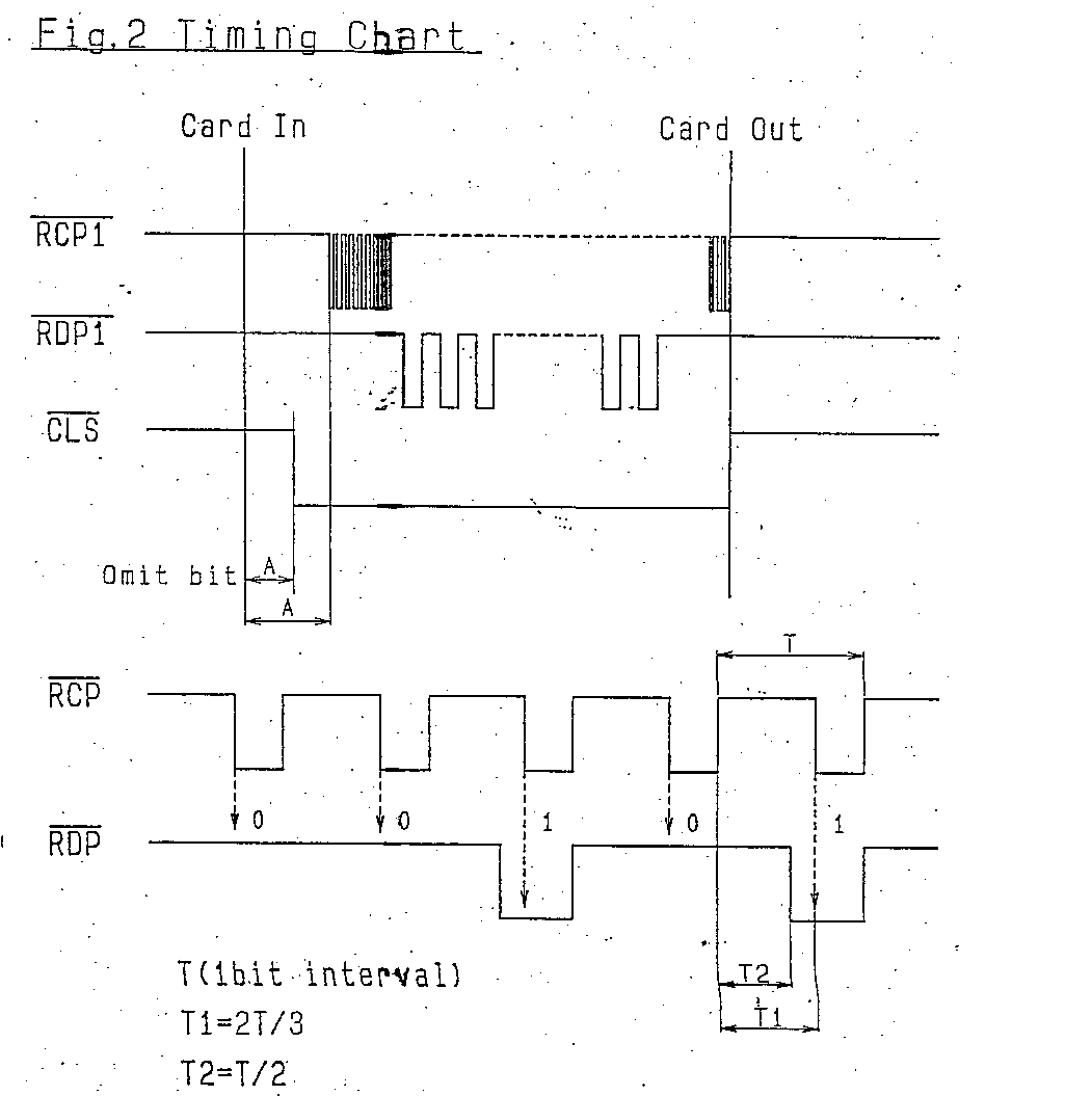
Magnetic Stripe Reader Timing
- The Magnetic Stripe Reader is
much like the LCD in that it has a series of signals, the important
signals on the magnetic stripe reader are: RCP, RDP, and CLS. It’s also
important to note that all three of these signals are inverted, this means
when one of the signals is toggled, it actually goes from high to low,
instead of low to high. The timing diagram below shows the value of RCP,
RDP, and CLS, not their complements as the label suggest. The timing for the signals is as
follows:
1. CLS is asserted (goes low) when the card enters the card reader.
2. At a later point RCP and RDP signals begin to be asserted. At the falling edge of RCP, RDP should be sampled for data.
3. RDP should be sampled at every negative edge of RCP, remember that RDP is inverted so if you sample a 0, it’s actually a 1 and vice versa.
4. Every 7 bits that you sample over RDP is a single ASCII character, you will have to decode it with the information found in the datasheets however. NOTE: You will be able to translate the 7-bit value to an ASCII byte in one statement.
5. RCP will stop oscillating when there is no more data to be sent. CLS will go back to high as well.
Use this information to draw a state diagram that you will code in Verilog to
read data from the magnetic stripe reader. Have your TA check this before you
move on. You will not need more than one state machine for this lab.
The Order of Data
- As you may have noticed already, data comes over RDP in a serial fashion, one bit at a time. The data comes over RDP in reverse order as well, the least significant bit first followed by the upper bits. There are a total of 7 bits per character; but the last bit (the highest order bit) is a parity bit so you can ignore it. There are several special characters as well, such as the start sentinel: 1000101, this start sentinel tells you when valid data begins. You should refer to the Reference Table for the exact encoding of all the supported characters. Take the time to look at the LCD encoding and the magnetic stripe encoding and determine what you need to do to the data from the magnetic stripe reader in order for the LCD to recognize it. You will have to code this into your Verilog module later on.
Asynchronous Inputs
- The signals from the magnetic stripe reader are not synchronous to our clock, meaning they can change anytime, even right when our clock is "ticking". This means, that if we sample one of these signals with a register, we could violate the setup/hold time constraints of the register. There are many ways to solve this problem, but they all use synchronizing flip-flops in the design. In other words, wherever you have inputs crossing clock boundaries that could cause setup/hold violations, you must place 2 flip-flops in series on the problematic signal and use the output of the second flip-flop as your input signal.
Building the Logic
- Now you are ready to actually
create the actual logic that makes the magnetic card reader work in
conjunction with your LCD logic. First off you should create a new design
for Lab 9 that has design flow since you will be synthesizing it onto the
FPGA eventually. You will have to add copies of the files from lab 8 that
controlled the logic of your LCD. If you want you can even rename the
copied over block diagram file from lab_8.bde to lab_9.bde. From there you
will want to remove the inputs you had added for the switches. You need to
add new inputs for CLS, RDP and RCP because that’s the signals coming from
the magnetic card reader.
Next you need to write up the Verilog code for your magnetic card reader logic. Don’t forget the logic that was explained above when you write your code. It should have a single 8-bit output, which you will direct to any inputs you had in lab_8 that was hooked up to the 8-bit switch input.
Testing your Logic:
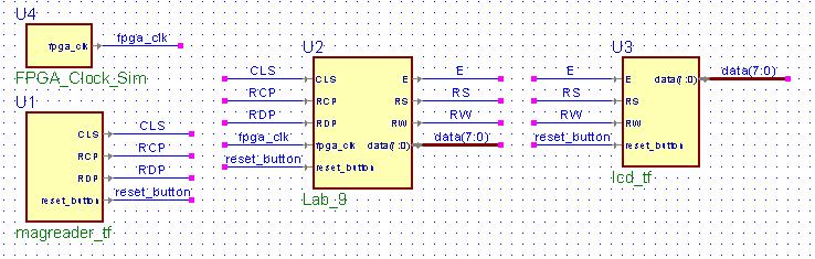
- A test fixture has been provided for you that will provide all the signals, all you need to do is hook it up appropriately. You can download the two test fixtures here: magreader_tf.v and lcd_tf.v. You can refer to the picture below on how to wire up your test fixture. Run the test and make sure everything passes successfully. The test fixture should print HOORAY!1+1=2 twice. If it does you are now ready to synthesize and demonstrate.
Synthesizing and Wiring:
- Now that you have tested your circuit and everything seems to be working it is time to synthesize it onto the FPGA and demonstrate it to the TA. Don’t forget to write up your .qsf file. You may be curious as to how you will get external signals like the LCD and Magnetic Card Reader to the FPGA. Well the I/O ports that you used in the earlier labs directly connect to the FPGA via the pin names on the label. This means inside your .qsf file you can assign the inputs from the magnetic card reader and outputs to the LCD to the I/O ports on your prototyping board via the pin labels on the label. You can refer to this page: IO Pins, if you are confused. What’s more, you can choose any I/O port you like in any order, which can make wiring very easy. Note that once you overwrite the default CSE370 program on the FPGA, these pins on the breadboard will no longer correspond to the switches, buttons or LEDs. For example, pin A13 will not be mapped to switch 9 once your logic is programmed onto the FGPA (unless you assign the pins that way yourself). Take a look at the TA’s sample solution below. That’s very clean wiring isn’t it?
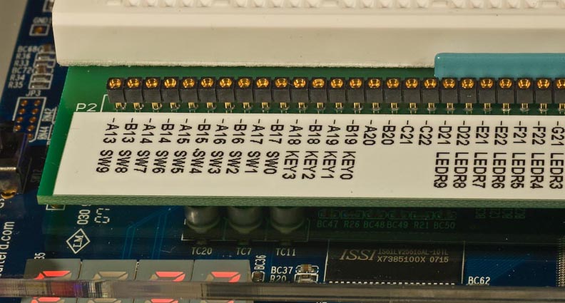
IO Ports, A13, B13, etc...
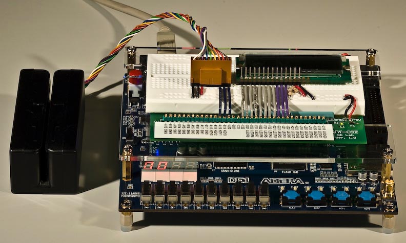
Good Wiring Example
Remember, the pin-outs described in the documentation are wrong. You should use
the following pin-out below when wiring up your magnetic card reader to the I/O
ports on your prototyping board.
|
Pin Number |
Color |
Signal |
|
1 |
White |
Frame GND (0) |
|
2 |
Grey |
Signal GND (0) |
|
3 |
Purple |
VCC (1) |
|
4 |
Blue |
RDP2 |
|
5 |
Green |
RCP2 |
|
6 |
Yellow |
CLS2 |
|
7 |
|
RDP1 |
|
8 |
Red |
RCP1 |
|
9 |
Brown |
CLS1 |
Additional Functionality (to make up lost lab points or just for fun!)
There are several extra credit
options you can undertake, these can be fun expansions to your learning if you
want to try them out.
1. Expand the logic of your magnetic card reader so that it can also make use
of RCP2, RDP2, and CLS2. This is the second track of the magnetic cards (The
same track your Husky Card uses). You will probably want to refer to this: Datasheet, for the encoding. In this case,
we suggest you set up a switch that is low for Track 1 and high for Track 2.
2. Most cards have 3 fields, one that stores the name, one for the credit card
number, and one for other data. There is a '^' character between each of these
fields. Hook up three switches and only print a given field if the switch
corresponding to that field is on. Do not print the start sentinel, end
sentinel, or field separators. Also don't print anything after the end
sentinel.
3. Include error checking into your magnetic card reader and LCD logic. Right
now everything should be built to spec and it works perfectly when the
conditions are right. However, it would be nice if the LCD would display an
error in the case the card in the reader is suddenly removed. See if you can
think of some ways to implement error checking.
Lab Demonstration/Turn-In Requirements
A TA needs to "Check You Off" for each of the tasks listed below.
- Have a TA check you off for your Magnetic Card Reader State Diagram.
- Have a TA check you off for your working Magnetic Card Reader with LCD.
Comments to: cse370-webmaster@cs.washington.edu