CSE370 Assignment 7
Distributed: May
12, 2010
Due: May 17, 2010 (start of class)
Reading
Review Katz/Borriello, Contemporary Logic Design 2e, Chapter 7
Exercises:
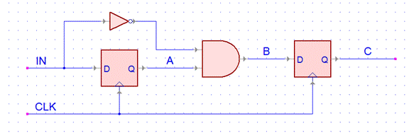
- Shown below is a simple
circuit along with a timing diagram.
Complete the timing diagram (using
this page) given the following values for the gate and register
parameters:
Registers: tpd = 2ns, th = 2ns, tsu = 2ns AND and INVERTER: tpd = 1ns
What is the “slack” time for this circuit?
That is, how much delay could be added to the critical path without violating a timing constraint?
Which timing constraint is first violated as delay is added?
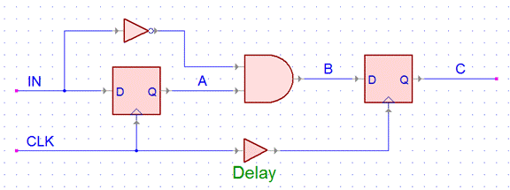
- Below is the same circuit
with a delay inserted in the clock.
This delay introduces “skew” between the clocks to the two
registers so that the clock edge does not arrive at the same time at each
register. Given a skew delay of
4ns, complete the next timing diagram (on
this page).
Are any timing constraints violated?
How does this change the operation of the circuit (ignoring timing constraints)? Explain what happened.
Let’s say you’ve already blown $5,000,000 making this chip. How could you get this circuit to work?
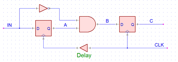
- Now change the skew delay to
2ns and complete the next timing diagram.
How does this change the operation of the circuit?
Are any timing constraints violated?
- Here is the same circuit but
with the clock skew delay in the opposite direction. Given a clock skew of 4ns, complete the
next timing diagram.
Are any timing constraints violated?
If you’ve already made the chip, how could you get the circuit to work? (i.e. avoid violating timing constraints)
- An arbiter circuit is used to
govern the use of a resource that is shared by more than one user. Each user signals that it wants to use
the resource by raising a Request signal.
The arbiter looks at the Requests that are being asserted and picks
one and raises the corresponding Acknowledge signal. When the user has finished using the
resource, it lowers the Request, and the arbiter lowers the Acknowledge
and repeats the process. This is a
synchronous process: the arbiter samples the Requests on the clock edge
and makes the decision. The
following timing diagram gives an example for two users. Note that the arbiter is fair: that is,
if both users request at the same time, the user who used the resource
last loses and the other user gets to go first.
Implement this arbiter using an FSM. First draw a state diagram, then the state transition table and finally come up with the next state and output functions. Draw a simple block diagram that shows the implementation of your state machine. You do *not* have to draw gates. You can just draw a box with the Boolean function.

- In this next problem, you will continue the design of a simple processor. You have already designed the register file and ALU. Now you will add a simple controller that can execute very simple programs. The text fixture for the register file from HW6 executed ALU commands that read values from two registers and stored the result value back to a register. We will now make our own controller that contains instructions that are executed on this simple datapath (ALU + register file), one at a time in sequence.
The figure below shows our simple controller, which uses a ROM (the iram module) to generate the control signals for the datapath. The PC0 module (program counter) is a simple counter that starts at 0 on reset, and then increments each clock cycle. Together these implement a simple state machine that starts in state ‘0’ and progresses through state ‘1’, ‘2’, etc. executing an ALU operation in each state. That is, the iram contains a simple program of instructions that are executed one at a time.
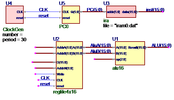

The iram is a table of 16-bit “instructions” in binary, whose format is shown above. RA, RB and RD are the addresses of the A and B source registers of the D destination register. Note that these are 3-bit values, but since we have only 4 registers in the register file (for now), we will use only the two low-order bits. The ALU Op is the opcode you used in the design of your ALU.
Construct the simple processor shown above using these files. You will have to add your register file and ALU to this. The file iram0.dat is a text file that is read automatically by the simulator to initialize the values in the ROM. The first few instructions are listed below. This program implements doubling, although not particularly efficiently. The file must be in the design folder, i.e. the parent of the src folder. Use this program to test out your processor design.
If your ALU or register file is not working, you can use the versions in this ZIP file.
10110_000_00_000_000 // R0 = 0
10010_001_00_000_000 // R1 = R0 + 1
10011_010_00_001_000 // R2 = R1
10000_001_00_001_010 // R1 = R1 + R2
10011_010_00_001_000 // R2 = R1
10000_001_00_001_010 // R1 = R1 + R2
10011_010_00_001_000 // R2 = R1
10000_001_00_001_010 // R1 = R1 + R2
10011_010_00_001_000 // R2 = R1
Write your own program in a new file that computes
the successive squares: 1, 4, 9, 16, 25, 36, … Hint: There is a smart way to do
this, so think first!
The file name is a parameter of the iram module – right-click the module to
change the parameter and then recompile.
Turn in the following for this problem:
1) Schematic of your simple processor
2) Printout of your program that generates the squares
3) Timing diagram of the program running, showing the values of the registers
in the register file