CSE370 Assignment 6
Distributed: May 5,
2010
Due: May 12, 2010
Reading:
- Review Katz/Borriello, Contemporary Logic Design 2e,
Chapter 6 (pp. 259-298).
- Katz/Borriello, Contemporary Logic Design 2e, Chapter 7
(pp. 307-347).
Exercises:
The test fixtures for this homework are linked here and are in the course hw6 folder.
In this assignment, you will continue the design of components for a simple processor. In this assignment you will add a register file memory to the ALU you’ve already designed. We will post a solution to the ALU design which you can use if did not get yours to work.
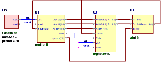
1. You have already designed the most complex component of your processor, the ALU. When the ALU performs an operation, it needs two values for input and a place to store the output. These values will be saved in the registers in what is called a register file. Our register file contains four 16-bit registers numbered 0 to 3. The ALU reads the values from two of these registers and the result is written back to a third. This register file is shown in the figure below labeled regfile4x16. The two addresses AddrA and AddrB indicate which register values are read to the A and B outputs, and AddrW indicates which register is to be written with the value on the D input. This register is written, at the clock edge, only if the Write input signal is asserted. The synchronous reset signal clears the registers in the register file to 0.
Design and test this register file using an Active-HDL schematic. Do not use Verilog for this design. The test fixture tests your register file and ALU working together as shown below. On each clock cycle, it specifies an op-code for the ALU and three register addresses for the register file and then makes sure that the result from the ALU is correct. You must change the clock period of the ClockGen to 30ns to give the circuit enough time. To do this, right-click on ClockGen, choose the Properties option and set the actual value of the parameter called "period" to 30. (You have to recompile of course.)
To implement this register file, you will need to make 16 copies of
components like registers. You can do this by actually making 16 copies using
cut-and-paste. (Make the lower bit first with all the signals connected, then
copy the whole thing.) But it is easier to use the ARRAY feature.
Right click on the component you want to “stack”, and enter the number of
copies you need. Turn on the ARRAY text parameter so you know you've made
an array of 16 copies.
WARNING: Don't use ARRAYs inside of ARRAYs
- there's a bug in the simulator that causes errors sometimes if you do
this. Also, use only simple arrays –
it’s easy to get confused if you try to push the idea too far.
If you are worried about your ALU design, we will post a solution that you can use by the end of the week.
2. The test fixture for the register file executes “instructions” which tell the ALU what operation to perform and which registers to use for the inputs and output of the operation. Single-step your test fixture (set the simulation time to 30ns., that is, the clock period), and write down what is executed by the test fixture for the first 10 clock periods. You should make a table that looks as follows. Show the values of the registers during the step, not after the result is written back to the register file.
|
Step |
reset |
R0 |
R1 |
R2 |
R3 |
Op code |
AddrA |
A |
AddrB |
B |
AddrW |
Result |
Write |
|
0 |
|
|
|
|
|
|
|
|
|
|
|
|
|
|
1 |
|
|
|
|
|
|
|
|
|
|
|
|
|
|
2 |
|
|
|
|
|
|
|
|
|
|
|
|
|
|
3 |
|
|
|
|
|
|
|
|
|
|
|
|
|
3. Design a BCD digit counter called bcdCount using Verilog. This is a 4-bit counter that counts from 0 to 9. It includes a synchronous reset and a cen (count enable) input, and a tc (terminal count) output, which is asserted when the count is 9. The TC output can be used to enable the next digit so that a two-digit counter will count 08, 09, 10, 11, …
We have provided a test fixture that instantiates 2 copies of your digit counter and tests to make sure it works. Note that you do *not* need to implement a top level schematic for this – the test fixture is the test fixture. Make sure you use signal and module names as described above. Turn in your Verilog code and the console showing the result of a successful simulation.
Rationale:
- To begin understanding the basic building blocks of
sequential circuits.
- To start designing and using sequential circuit
building blocks.
- Start to familiarize yourself with the finite state
machine design and implementation process.