CSE370 Assignment 5
Distributed: April 28, 2010
Due: May 5, 2010
- Katz/Borriello, Contemporary
Logic Design 2e, Chapter 5, Section 5.6
- Katz/Borriello, Contemporary Logic
Design 2e, Chapter 6
Exercises:
All the files you will need for this homework can be found in this ZIP file.
1. By the end of the quarter, you
will have designed yourself a simple processor.
The first component of that processor is an ALU that you will design
here. Make sure you keep this design so
you can use it later.
Using Active-HDL, design and test a 16-bit ALU
that executes the functions described in the following table. The OP Code
has three bits and tells the ALU which operation to perform on the two inputs,
A and B. Note that only six of the possible eight OP codes are used.
|
Operation |
ALU result |
OP Code |
|
ADD |
A + B |
0 |
|
SUB |
B - A |
6 |
|
INC |
A + 1 |
2 |
|
Pass A |
A |
3 |
|
XOR |
A XOR B |
1 |
|
XNOR |
A XNOR B |
5 |
Design your ALU using a bit-slice approach.
That is, design a single bit of the ALU that can be copied N times to
create an N-bit ALU. You should
start with the carry-lookahead adder you designed for the last homework, and
just replace the 1-bit adder with the ALU slice you design here.
The carry-lookahead part of that circuit will compute all the carries for
you. You should be able to implement
the functions given here using that ALU. Although we have chosen the OP
Code to make things somewhat easy, you will have to convert this 3-bit OP Code
defined here into the control bits that your ALU needs. (If you were not able to get a working
carry-lookahead adder for the previous homework, we will give you a working
solution.)
You may add extra functionality to your ALU by
increasing the number of op codes and op code bits. If you do this, then
you will also have to extend the test fixture to handle your ALU - I can help
you with this if you decide to go this route.
Turn in a printout of your design along with the
screenshot of the console running the test fixture.
2. Check out the problem2 design files. This
is your first circuit with a register in it. Run this circuit by
executing in steps of 5ns. What does this circuit do? Modify this
circuit so that it produces a 1 on the output when it sees 4 consecutives 1's
on the input. Test using the test fixture problem2a_tf. Hand in a
screen shot of your circuit along with the console showing that your circuit
works.
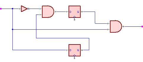
3. Complete the timing diagram below for the
following circuit using hand simulation. Assume that gates and inverters have a
delay of 1ns, and that the propagation delay of the register is 2ns. The
vertical lines mark 1ns time; thus the clock cycle is 10ns.
1.

a) Draw a state diagram that describes the
operation of this circuit.
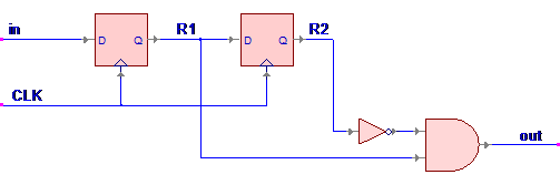
4. Draw the state diagram corresponding to the following circuit.