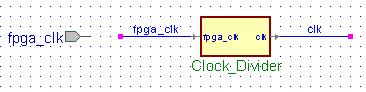
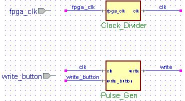
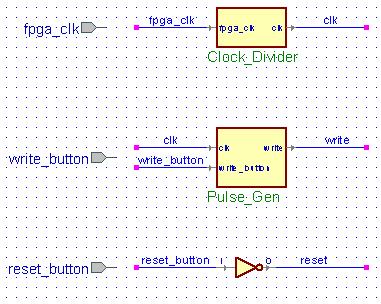
The Clock:
If this is the problem, then how do we solve this problem? The most logical way would be to slow down the clock since we have no control over the internals of the LCD. Look at the provided clock_divider.v file, this verilog file divides down the clockspeed inputted into it and outputs a slower clock. Make sure you understand how it works because it is incomplete. Change the bits parameter and and the ratio parameter by filling in values for the x's such that it slows down the clock enough for the LCD to run properly. Have your TA check you off to confirm that you have an acceptable clock speed.
The Write Button:
The Reset Button:
The LCD:
| Pin | Name | Function |
| 1 | GND | Ground - wire GND to it |
| 2 | VDD | 5V - Powers the LCD, wire the 5V red VDD to it |
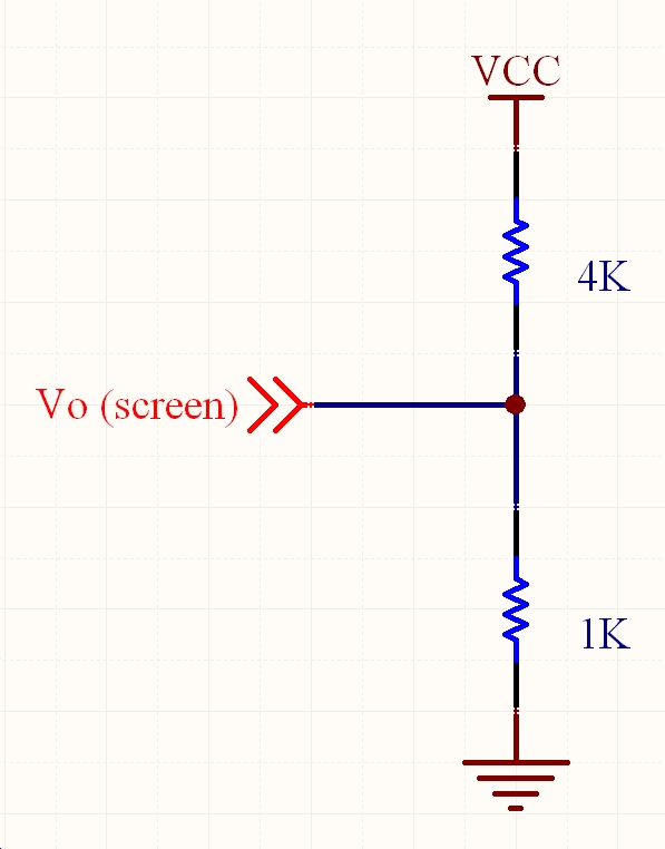
| 3 | Vo | 1V - Contrast, The LCD needs exactly 1V on this pin so characters are visible |
| 4 | RS | High: When RS is high the LCD expects
data to come over the data pins Low: When RS is low the LCD expects one of the hard-encoded commands to come over the data pins |
| 5 | R/W | High: When R/W is high the LCD can be
read from Low: When R/W is low the LCD can be written to |
| 6 | E | This is the Enable, it executes command/data is passed to the LCD on the negative edge of E |
| 7 | DB0 | Data Bus 0, this is one bit of data |
| 8 | DB1 | Data Bus 1, this is one bit of data |
| 9 | DB2 | Data Bus 2, this is one bit of data |
| 10 | DB3 | Data Bus 3, this is one bit of data |
| 11 | DB4 | Data Bus 4, this is one bit of data |
| 12 | DB5 | Data Bus 5, this is one bit of data |
| 13 | DB6 | Data Bus 6, this is one bit of data |
| 14 | DB7 | Data Bus 7, this data bit also acts as an output for the LCD. When R/W is high and RS is low, the LCD will output a high signal if the LCD is busy and low signal if the LCD is not busy. |
LCD Control Logic:
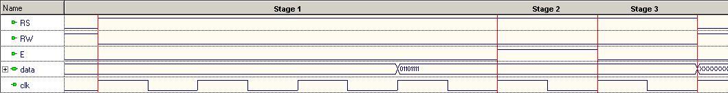
Checking Busy Signal Waveform:
 | |||
|
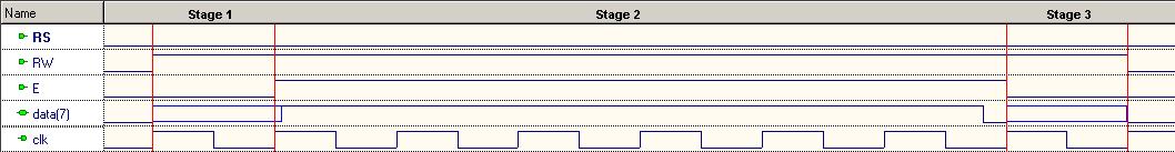
Command/Character Write Waveform:
 | |||
|
LCD Setup Commands:
| Order | Operation | RS | DB[7:0] |
| 1 | Clear Display | 0 | 0000 0001 |
| 2 | Function Set | 0 | 0011 0011 |
| 3 | Display On | 0 | 0000 1100 |
| 4 | Entry Mode Set | 0 | 0000 0110 |
| 5+ | Write Character | 1 | ???? ???? |
Before you write any character or command to the LCD you must check the busy signal first. In fact your circiut should always be alternating between checking the busy signal and writing something to the LCD. A state machine is a very good way to control what stage of the above waveforms you are in. You should also think about making a state machine to keep track of what command you are on or whether you've finished sending the commands and are now sending characters. Note that for every command/character the second state machine goes through, the first state machine must complete a full cycle. This means that the first state machine must have an output that is used as an input to the second state machine. Also note that because there is not a steady stream of characters to write there will be times when you will have to wait in stage 1 of the write waveform. Whether or not to pause is something the second state machine must tell the first. There is also the question of how to deal with RS because its value depends on the state of both machines. Based on the information that you have now, you should be able to design two simple state machines/state diagrams that carry out all of the logic described above. Show your TA your completed state diagrams before moving on.
Programming States in Verilog:
|
module case_state_example (CLK, Next, Reset, Fib_Out);
input CLK, Next, Reset; output reg [4:0] Fib_Out; reg [2:0] state; intial state=0; always @(posedge CLK) begin if (Reset) state = 0; else case (state) 0: if (Next) state = 1; 1: if (Next) state = 2; 2: if (Next) state = 3; 3: if (Next) state = 4; 4: if (Next) state = 5; 5: if (Next) state = 6; 6: if (Next) state = 7; 7: if (Next) state = 0; endcase end always @(state) begin case (state) 0: Fib_Out = 1; 1: Fib_Out = 1; 2: Fib_Out = 2; 3: Fib_Out = 3; 4: Fib_Out = 5; 5: Fib_Out = 8; 6: Fib_Out = 13; 7: Fib_Out = 21; endcase end endmodule |
If you look over the code, it is actually very redundant, the output given is just the next Fibonacci number in the sequence, which resets or cycles back to the first Fibonacci number. The technique is relatively simple, you only need a register to remember which state you are in, and then a case statement that determines the logic to advance states. You can include an intial block as well to state what value the registers begin with. Another always block can be used to change the output based on the changing state, as the second always block demonstrates in the code. You can use this system to write the logic for your LCD.
Tri-State Command and Data:
|
input Select; input [7:0] Data; output [7:0] DataBus; assign DataBus = (Select) ? Data : 8'zzzzzzzz; |
As you can see from the code above, the Select input acts just like a multiplexer, choosing from the Data that comes in or the high impedance z signal. A good example of tri-state is the LCD that you are working with. Since the LCD can both output a busy signal and take in a command/character you know it is tri-stating between those two possibilities. Since the LCD is expecting either input or output you need to write your code so that it can handle this case. Sometimes you will be taking an input from the LCD checking for a busy signal. Other times you will be passing either a command or character to the LCD. Since you switch between output and input, you're going to have to tri-state. HINT: In the case of this project, your tri-state is probably based off RW because it controls whether you are reading or writing.
In-Out Buses/Wires

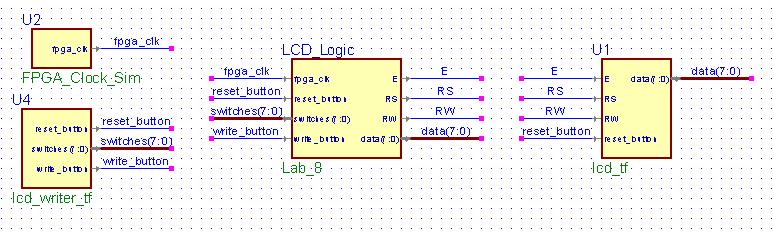
Testing Your Logic:
fpga_clock_sim.v
lcd_writer_tf.v
lcd_tf.v
Make sure that the expected message prints out: "Hooray!".