CSE 370 Introductory Laboratory Assignment

Making a Full Adder with a Multiplexer, Decoder, and PAL (Programmable Array Logic)


Assigned: Monday, October 22, 2007
Due: End of Lab Section


Objectives

In this laboratory assignment you will learn to use multiplexers, decoders, and PALs to create a full adder. If you haven’t covered multiplexers or decoders in class yet you can refer to Chapter 4 of Contemporary Logic Design. We will provide you with a brief summary of PALs are and what they can do in this lab, however you can also refer to Chapter 4 of your textbook for more information.

The PAL (Programmable Array Logic) chip that we will be using in this class is designated as a 22V10 (here is a functional logic diagram if you’re interested). This is a very flexible PAL that you will be using in different ways this quarter. At the core of this PAL are 10 logic blocks that each computes a Boolean function. This output can either go straight to a pin or through a register to a pin. We are concerned only with combinational logic right now, so we will ignore the register. The output also feeds back into the PAL, so that you can use it to implement multi-level logic functions.

This is how this PAL gets its name: functions of up to 22 inputs, with 10 distinct outputs, hence, 22V10. Note: for now, ignore the other logic elements in this PAL, we'll come back to them later in the quarter. After you familiarize yourself with the component, you will write some Verilog code that will be compiled into the logic in this PAL. This is yet another useful capability of the ActiveHDL tool. For this lab we will be using the module you designed in the previous lab assignment. You can map your design onto the PAL with the provided software at the mapping terminals by the door of the lab.

Before You Begin

Before you begin this lab you will need to have two things ready:
  1. Your verilog implementation/design of a full adder from Lab 3.
  2. The verilog full adder test fixture (FA_tf.v) from Tutorial 3 in Lab 3.
Remember when you are designing your decoder and multiplexer design of the full adder you only use the C74 chip packages included in the lib370 library. An example is provided below.

Notice that the chips in the cse370 library need to be powered just like real world chips. That is why there is a VCC connection and a GND connection in the picture. Be sure you connect up the right ports! You can always look on your chip maps if you are unsure about anything.

***NOTE
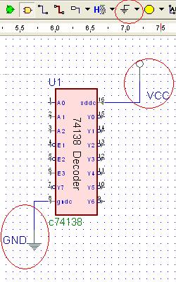
If you look on the chip you will see a few inputs called E1, E2, and E3. These are the enables, you need to use these to turn on and off the chip. Enables aren't too complicated though they are difficult to understand at first. Enables are like the power switch to the chip. If any of them are disabled the chip won't perform correctly, just like a computer won't work if you don't turn it on first.

Like with most electronics the enable is only considered "ON" when the chip sees the input to be a 1. Of course that means you generally have to connect up VCC to it so that the Enables are read as being "ON" or being a "1". However, sometimes if you look on the chipmap you will see that there is a little bar over the E. This means that the input is inverted, whatever goes in is flipped. In this case if you hooked up VCC, it would get inverted to GND and the chip still wouldn't work. In the case where there is a little bar you should hook up GND so that when it is inverted it is read as a "1" or "ON". Keep that in mind and everything should work well!

Tasks

    Part 1: Can be done outside of Lab Time
  1. Your first task is to implement a full adder with a 3:8 decoder (‘138 chip) as your primary piece of logic. When you design your full adder in Active-HDL don’t forget to use the C74 chips provided for you in the lib370 library. It will make building your designs a lot easier later on. Don’t forget to apply what you’ve learned in class such as deMorgan’s law to pick the right sets of chips. Also don’t forget to set the correct Enables on the chips in the design. Refer back to the part in the lab about Enables if you skipped it, or I suppose you could ask a TA.

    When you think you have provided a working design test it with the provided test fixture from Lab 3. It is linked here: FA_tf.v. You don’t have to hand in your test diagram, but we do need to see it. Call over a TA so they can check you off for this first part. Remember to check to make sure your test fixture actually passed with the right results. If you see X’s you did something wrong.

  2. Your second task is to implement a full adder with one 4:1 multiplexer (‘153 chip) for each output that you need to compute (sum and carry-out are the two outputs you need to compute). You can use any other necessary chips such as inverters to implement your full-adder. To save you some wiring you should see that the (‘153) contains two 4:1 multiplexers so you should only need to have one 153 chip placed on your prototype board. As a reminder again, use the C74153 chip in the 370lib when you design it in Active-HDL. You should not be using the included multiplexers in Active-HDL.

    When you think you have provided a working design test it with the provided test fixture from Lab 3. It is linked here: FA_tf.v. Once again, if it is working and you don’t have strange outputs like X’s, you should call over a TA so that they can check off your design.

  3. Your third task is to take some time to familiarize yourself with the 22V10 functional logic diagram. Make sure you see how the logic functions are computed in the component. If you don’t understand you can always refer to Chapter 4. It is important that you understand PALs at this point because you will have homeworks and additional labs involving them.
  4. Part 2: Needs to be done during Lab Time
  5. Complete the entire PAL Tutorial that explains how to compile a circuit into a PAL using Active-HDL and the Cypress compiler. Once you have completed the tutorial you should compile your full-adder Verilog module from your previous lab and program it into a PAL using the PAL programming stations in the lab by the door. In case you don’t know what the PAL looks like, they are longer chips with the 22v10 labeled on them. You should have 3 of them in your kit. ***Note: You should check to make sure you are saving the compiled version for the PAL on a network drive that can be accessed from a different computer. That means saving on your desktop won’t work.

  6. After you program your PAL, you need to wire it up on your circuit board and use switches and LEDs as inputs and outputs. Use SW0 for A, SW1 for B, and SW3 for Cin and LED0 for Sum and LED1 for Cout. Make sure that your full adder operates correctly. Don’t forget to leave room for your multiplexer chip as well on your breadboard, you will need to implement them as well. In case you don’t know how to wire up your PAL you should carefully read over the report that is generated by Active-HDL when you compile for the PAL. It contains a lot of detailed and useful information.

  7. Now wire up your multiplexer implementation of your full adder using the same switches for A, B, and Cout so that your PAL and Multiplexer will get the same inputs at the same time. However this time you should use LED2 for Sum and LED3 for Cout. Once you have both of the implementations working you should demonstrate it to the TAs for a final checkoff.

Lab Demonstration/Turn-In Requirements

A TA needs to "Check You Off" for each of the tasks listed below.
  1. Show your decoder implementation using c74XXX gates in Active-HDL to a TA.
  2. Show your multiplexer implementation using c74XXX gates in Active-HDL to a TA.
  3. Demonstrate both the PAL and multiplexer implementations on your prototyping board.

Comments to: cse370- webmaster@cs.washington.edu