Introduction to Active-HDL
Tutorial #1 – Creating and
Simulating Simple Schematics
This tutorial will introduce the tools and techniques
necessary to design a basic schematic. The goal of this tutorial is to
familiarize you with Active-
·
Start Active-
· Create a new workspace and design
· Add and remove files to and from a design.
· Place parts in a schematic design from the built-in library.
· Use wires in a schematic design.
· Run a basic simulation.
· Debug a schematic design.
Even though this tutorial will show you all you need to know
to do basic designs and complete the assignment, you should experiment with
Active-
Start
Active-
First, start Active-
NOTE: If you already have a
Workspace you can skip to Create a New Design
Create a new
workspace
A workspace holds your designs, and
each design may consist of many files (i.e. schematics, Verilog source code,
etc). When you open Active-
- Select the “Create new workspace” option. This opens the New Workspace window:
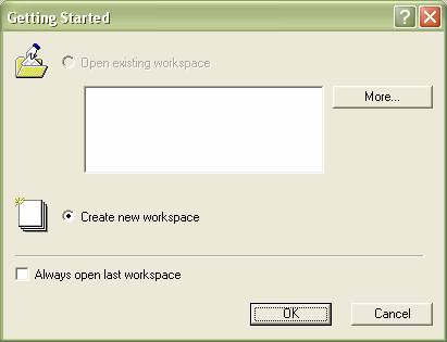
Figure 1
- Enter a descriptive name into the “Type the workspace name field.
- Change the workspace directory by entering it in the “Select the location of the workspace folder” field, or use the “Browse” button to select the new directory. We strongly recommend you use your student drive. Note: Files saved to the local drive will be automatically deleted on logout.
- Select the “Add New Design to Workspace” check box if it is not already checked.
- Your New Workspace window should look like Figure 2. If so, click the OK button, and continue.
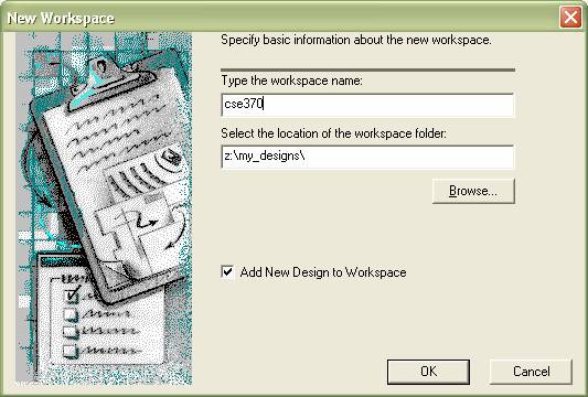
Figure 2
Create a design
If you just completed creating a workspace and if you check the box “Add New Design to Workspace” in the New Workspace Wizard the New Design Wizard will automatically start. Otherwise you will need to select a new design from the File menu.
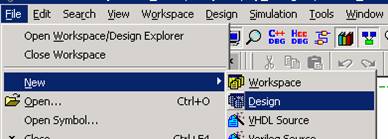
Figure 3
The New Design Wizard walks you through creating a design. A design can consist of one or more Verilog modules, schematics, and other design files. A workspace, as mentioned earlier, can contain one or more designs. You can add more designs later by selecting File/New/Design in the menu bar. For now, we will add the first design to the workspace by following the steps provided on the following pages.
1. Click the “Create an Empty Design with Design Flow” radio button. Then click the Next button.
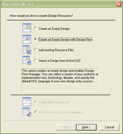
Figure 4
2.
Find the “Block Diagram
Configuration” field and select the “Default
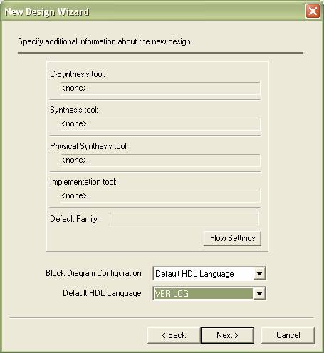
Figure 5
3. In the “Type the design name” field, type a name for your new design. The name must contain only letters, numbers, and underscores (“_”), and cannot start with a number (i.e. 4bitadder is invalid, however four_bit_adder is valid). Use descriptive names that do not match file names, other design names, or workspace names. By default, the design directory is under the workspace directory, and the name of the default working library of the design is the same as the design name. Leave these default values alone. Warning: the directory path should not contain any spaces in it. Your window should look like 6 with a more descriptive name than “combo_logic”.
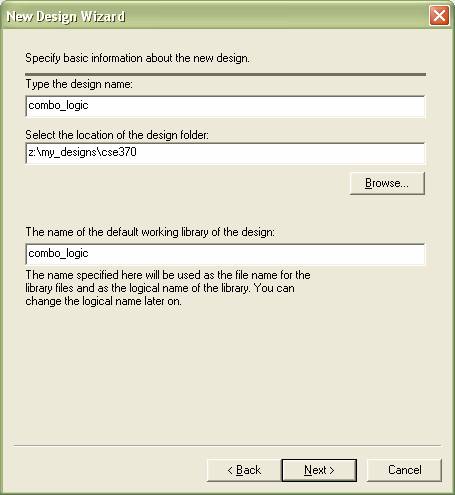
Figure 6
4. Double check your file name and location, then click the Next button.
5. Make sure that your design name is correct and the design directory is correct in the window that follows (not shown). If not, click the Back button to make any changes, or click the Finish button to create the design.
Add a Block Diagram (schematic) file
At this point your screen should look like Figure 4 (shown on the following page). The frame on the left is called the Design Browser and lists all of the components in your design. The frame on the bottom is the Console and is where status and error messages are printed. If these frames are not open, or if you have closed them by accident, you can open them by going to View in the menu bar. In the center of the screen is the main window where you will draw your schematics. When your design is first opened, the Design Flow Manager opens in this window. We won’t be using this tool during this tutorial. At the top of this window is the Standard toolbar. Finally, notice the tab at the bottom left side of the main window. As you create schematics and other components in your design, you can use the tabs at the bottom of this window to make the corresponding file active in the main window.
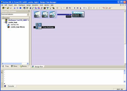
Figure 4
1. Double-click the “Add New File” option in the Design Browser (Figure 8). This will open the Add New File window.
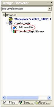
Figure 5
2. Click the Wizards tab in the Add New File window. Select the Block Diagram Wizard icon, and then click the OK button (Figure 9).
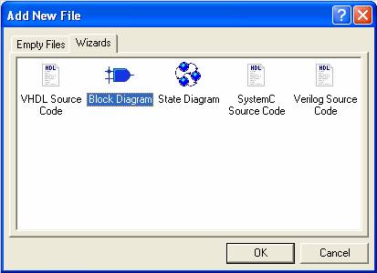
Figure 6
3. In the New Source File Wizard, make sure that the box is checked next to the “Add the generated file to the design” option. Click the Next button. Note: this window is not shown.
4. Select the “Verilog” option, and click the Next button (see Figure 7).
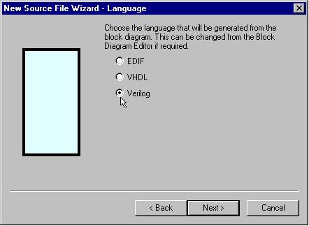
Figure 7
5. In
the “Type the name of the source file to create” field, enter the name of your
schematic design. Use descriptive names. Do not us the same name that
you named your design or workspace. Also, do not use a different name for
the module; leave this field blank. Active-
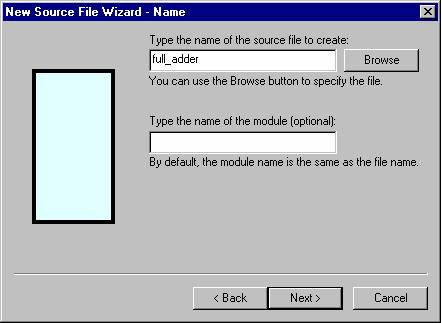
Figure 8
6. This window is where you add your input and output ports. You do not have to add any ports at this point in the design process; however, adding the ports now will save time. If you choose not to add any, click Finish and skip steps 7-9.
7. To add ports, click the “New” button. Choose whether you want an input or output port by clicking the desired radio button located under the “Port Direction” heading.
8. In the “Name” field, type the name of the port.
9. We will only be using 1-bit ports, so ignore the “Array Indexes” fields for now. Your screen should look like Figure 9. If so, then click the Finish button.
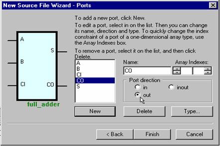
Figure 9
The wizard generates a schematic that is empty except for
any ports you specified in the design process (see Figure 10).
Notice this schematic file has been added to the design in the Design Browser
on the left. Schematic files in Active-
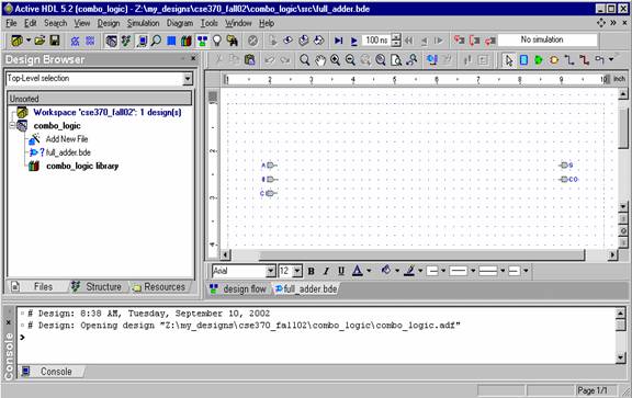
Figure 10
At some point, you may wish to detach files from your design, or delete them completely. You can do any of those tasks by simply right clicking the file in the Design Browser and selecting the “Remove” option from the pop-up menu. You will then be asked if you want to detach the file (remove it from the design without deleting it completely) or delete the file. Obviously there is a lot more that you can and may want to do to manage your files, but for now just get comfortable with these basic steps towards file management.
Place parts into your schematic design
Now you are ready to build your gate logic. The steps below
will teach you how to add basic gates to your schematic and how to add single
bit input and output terminals, in case you decided not to do so in the design
wizard process, or you realized that you are missing some terminals (Note:
this tutorial uses the icons in the toolbars and other shortcuts to access most
of the tools in Active-
Figure 11 is the final version of the schematic you will be drawing. Your final design should look similar*.
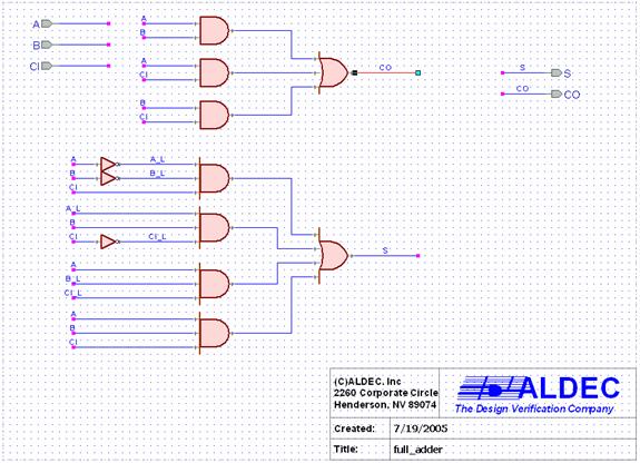
Figure 11
*Some
of the components you use may differ in appearance from the components shown in
this tutorial.
1. You are required to use the components located in the standard class library. Do not use built-in symbols. Therefore, you need to add the symbols for the components in the standard class library to the symbols toolbox using the Library Manager. Open the Library Manager by clicking the Library Manger icon in the toolbar (Figure 15).
![]()
Figure 12
2. Locate the lib370 library in the left frame of the main window, and right click it (Figure 16).
3. Select the “Add to Symbols Toolbox” option.
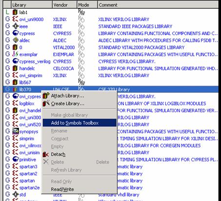
Figure 13
4. Close the Library Manger by clicking its icon in the toolbar, or select File/Close.
5. Open the Symbols Toolbox by clicking the Symbols Toolbox icon in the toolbar (Figure 17).
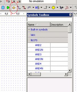
Figure 14
6. Click the plus symbol to the left of the “lib370” option to expand the list. Scroll down the to find the desired part from the list, or type in the name of the part in the field at the top of the Symbols Toolbox to search the list.
7. Click on the parts name in the list and notice that its symbol appears at the bottom of the Symbols Toolbox.
8. Add the part to your schematic by dragging the symbol from the Symbols Toolbox into your design.
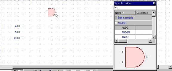
Figure 15
9. Active-
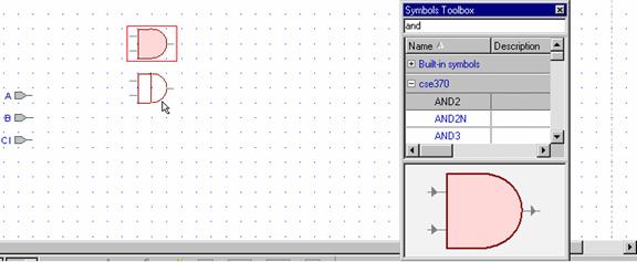
Figure 16
10. (Skip steps 6-8 if you added your terminals in the New Block Diagram Wizard) To add a terminal click the drop down arrow next to the Terminal icon in the toolbar (or click Diagram/Terminal in the menu bar). Click the “Input” or “Output” option in the expansion menu.
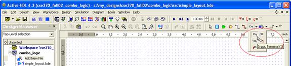
Figure 17
11. Click in the schematic where you want the terminal.
12. Notice that you can continue to click and add multiple terminals. To stop adding terminals, press the Esc key. Note: The Esc key is very useful to “get out” of just about any process (i.e. drawing wires, placing components, etc).
Moving gates and terminals is as easy as clicking and dragging the part to the new location. Additionally, the arrow keys are very useful for moving components precisely where you need them in the schematic. To delete parts, simply click the part to be deleted (when properly selected, the part will be outlined in a red box), and then press the Delete key.
In addition to moving and deleting gates, you may want to rotate and flip gates.
· Step 1: Select the part by clicking on it.
· Step 2: Then right click on the part.
· Step 3: In the pop-up menu, select the “Mirror” or “Rotate” options.
Using wires in Active-HDL
This part of the tutorial will show you how to make connections using wires, how to move the wires, how to name wires, and how to delete wires.
1. Click on the Wire icon in the toolbar (see Figure 18).
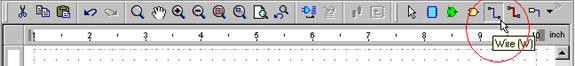
Figure 18
2. Now click anywhere in the schematic and drag your mouse to the point in the schematic where you want the wire to end. Clicking on a port or terminal will connect an end of the wire to that port or terminal, clicking on another wire will create a junction, clicking on an empty space in the schematic will create an anchor or bend in the wire at that point, and double-clicking an empty space in the schematic will create an end to the wire at that point.
3. When you are done placing wires, go back to select mode by pressing the Esc key or clicking the Select Mode button in the toolbar.
Removing wires:
1. Select the wire by clicking on it (the selected wire will turn red).
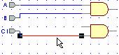
Figure 19
2. Press the Delete key.
Moving wires:
1. Click and drag on the wire or part of the wire to be moved.
2. Drag your mouse to the new location and release the button.
Naming wires:
1. Double-click the wire segment you wish to label. This opens the Wire Properties window (Figure 23).
2. In the “Segment” field under the General tab, type the name.
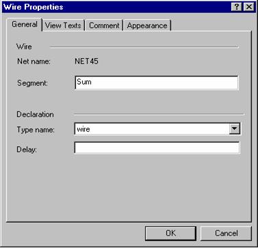
Figure 20
3. Click OK.
Connections to terminals can be made “by wire” or “by name”. By wire connections connect terminals by a wire. If a wire and a terminal have the same name, they are connected by name. Lots of wires can be confusing and named connections are used to make easy to read schematics. Figure 21 is an example of both methods. Also, the final schematic version of the full adder presented earlier (Figure 11) shows how to create an easy to read schematic using connections by name.
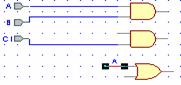
Figure 21
** Complete your schematic so it looks like Figure
11 **
Checking, saving, and compiling your design
At this point you should have a schematic with gates and terminals connected using wires. However, your file in the Design Browser is still preceded by a question mark. Before you can run simulations you need to compile your design, at which point the question mark will become a green check mark if all is well, or a red “x” if there are errors.
1. Always save your files first. To do this, click the Save icon in the toolbar, or press Ctrl-S with the file’s tab active in the main window. Remember to save early and often throughout the design process.
2. Active-
Figure 22
3. After
you have checked your diagram and resolved any errors or warnings, click the
Compile icon in the Standard toolbar. See the
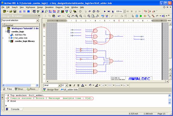
Figure 23
DRC Report
When you run the check diagram tool, a
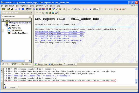
Figure 24
Simulating a design
To ensure that your design functions as you intend, you need to simulate it. This portion of the tutorial will show you how to set the top-level, how to open a waveform, how to add signals to a waveform, and how to use “stimulators”.
Important: close all open waveforms from previous simulations, if any, prior to running a new simulation.
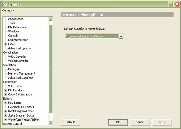
1. Before
starting the simulation you have to enable the “Standard Waveform
Viewer/Editor”. Under “Tools->Preferences” select “Waveform Viewer/Editor”
on the left and change the default editor to the “Standard Waveform
Viewer/Editor”.
2. Before
you can simulate a design, you must set the top-level. Since designs can be
composed of multiple files or layers, we need to tell Active-
Note: the following design entities are valid choices when setting the top-level: a configuration [“C” icon], a module [“M” icon], or an EDIF cell [“D” icon].
3. Right click the module.
4. Select the “Set as Top-Level” option. If you
do not set the top-level, Active-
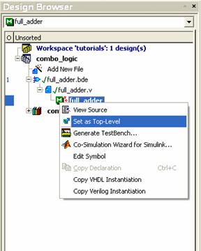
Figure 25
5. Select “Initialize Simulation” under Simulation in the menu bar.
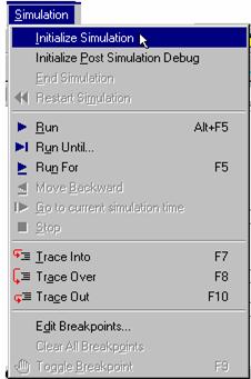
Figure 26
After selecting “Initialize Simulation”, notice in Figure 27 that the Structures tab is opened in the Design Browser.
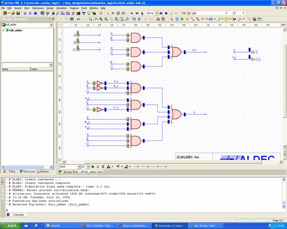
Figure 27
4. Click the New Waveform icon in the Standard toolbar.
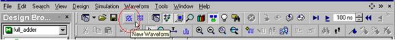
Figure 28
5. Click the file name in the top window in the Design Browser under the Structures tab. Notice in Figure 29 how the signals and wires (Nets) appear in the bottom window of the Design Browser.
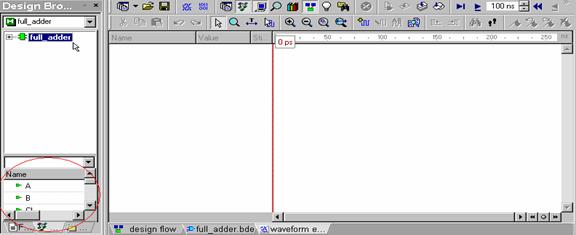
Figure 29
6. Add the signals to the waveform by dragging the signals one by one into the left side of the waveform. A faster method of adding signals to the waveform is to select the signals using the Shift or Ctrl keys. Now you may drag them as described above into the waveform. You can also right-click on a selected signal, and click the Add to waveform option in the pop-up menu as shown in Figure 30.
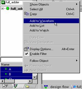
Figure 30
7. To
simulate a design, we have to provide values for the input signals. Active-
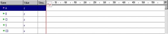
Figure 31
8. Click the “Stimulators” option in the pop-up menu.
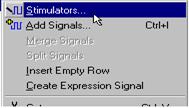
Figure 32
9. The Stimulators window will pop up with the Signals tab active. The large arrow points to a list of stimulators, and your signal is shown on the left side of the window in the signals field. The “Type” list shows the different stimulator options: choose the “Clock” option. See “Using Stimulators” at the end of this tutorial to learn about some of the other options.
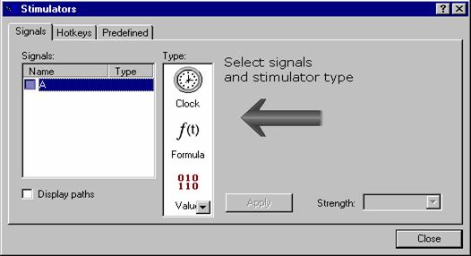
Figure 33
10. With the Stimulators window still opened, you can set additional signals by clicking the signals in the left side of the waveform. Once you have added all three input signals (i.e. A, B, and CI), choose a clock period of 10 ns for A by entering the time in second box from the left at the top of the window (see Figure 34). Click the Apply button.
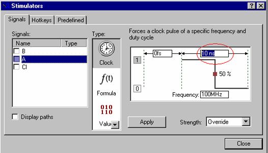
Figure 34
11. Select clocks with periods of 20 ns, and 40 ns for the other inputs.
12. When you are finished applying your stimulators, click the Close button.
At this point, you are ready to run the simulation using the waveform and stimulators.
1. The “Run For” field located in the Standard toolbar controls how long to run the simulation. You may change this by using the up and down arrows to the right of the field, or you may type in a time.
![]()
Figure 35
2. Click the Run For button in the Standard toolbar
![]()
Figure 36
3. To restart the simulation, click the Restart button in the Standard toolbar.
![]()
Figure 37
Note: if you make changes to the waveform by changing stimulators or adding/removing signals, you need to restart the simulation. Similarly, any changes in the file mean the file needs to be saved and recompiled prior to restarting the simulation. To end a simulation, simply click Simulation/End Simulation in the menu bar.
Figure 38 is an example of a simulation using the steps provided in this tutorial.
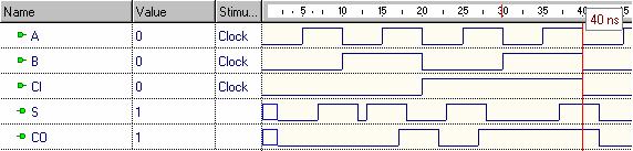
Figure 38
Now that you have ran a simulation and created a waveform, you should save that waveform. With the waveform tab active, press Ctrl-s to save, or right-click the tab and select save. Remember to use descriptive names. A good naming convention is <design name>_wv. This is the naming convention that will be used in the next assignment. For example, the waveform below would be saved as full_adder_wv.
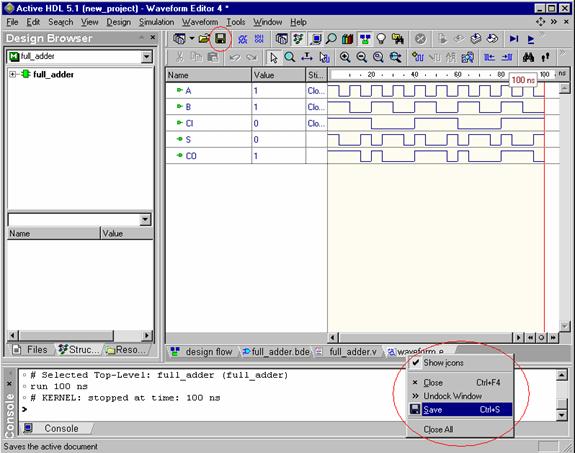
Figure 39
You may have several waveforms for the same design. This is very useful in comparing different signal values and methods of driving the input signals. However, you should close all waveforms when you are done to avoid confusing signals when simulating other designs. You should experiment with the different methods available and save the results in separate waveforms for comparison; however, this is optional.
Debugging a design
We will walk through a simple, yet common, scenario with a
schematic that contains errors and warnings. Some of these problems can be
pinpointed and solved by simply running a check diagram and reviewing the
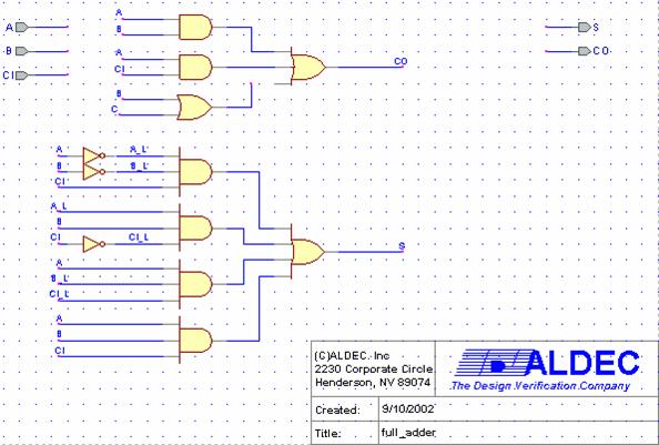
Figure 40
*This
schematic was designed using parts from the Built-in library. Therefore, there
are no gate delays.
- First,
we saved, and checked our design. When checking the schematic shown in Figure 40, Active-
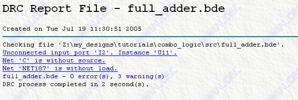
Figure 41
- Clicking on the first line took us to the broken connection on the 3-input OR gate. The part in question was highlighted in a red box (not shown here). Therefore, we simply reestablished the connection by dragging the hanging wire to the 3-input OR gate port (shown fixed in Figure 42).
- The
second warning showed that net ‘C’ was without a source. Again, we clicked
this hyperlink, and it took us to our schematic and highlighted the wire
named ‘C’ in red (see Figure
42). The connection looked
fine, but notice that we have no terminals by the name of ‘C’. The
terminal we wanted to connect from was ‘CI’. This kind of mistake is
common when using naming connections, and Active-
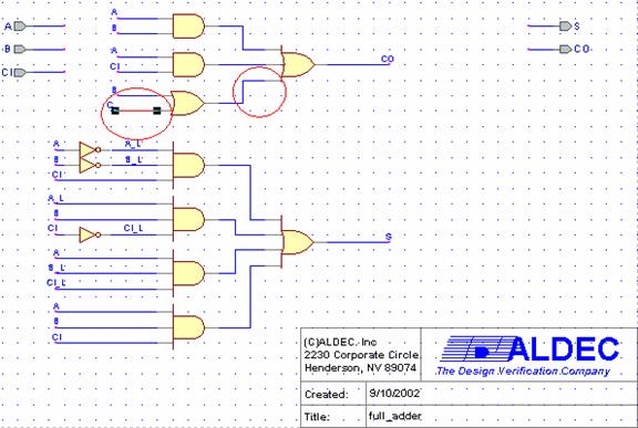
Figure 42
4.
After we had corrected the first two warnings, we clicked on the third.
This hyperlink took us to our schematic and highlighted the segment that was
broken earlier, but we had already fixed it in the second step. This could have
meant there was another problem with this segment, or the problem was that this
broken connection had raised two errors involving the two gates. At this point,
we saved the file, and ran the check diagram tool again. Figure 43 shows the results of this DRC report, and according to
Active-HDL all was well.
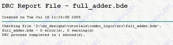
Figure 43
- Now we compiled the design, and it compiled successfully. Therefore, we initialized a simulation, added the signals to a waveform, provided clock stimulators for the signals, and simulated the design. Figure 44 shows the results of this simulation. When comparing the waveform to the expected results (we used a truth table), everything looked fine until we got to the 10 to 15 ns period. The sum should have been 1 and the carryout should have been 0, but both were 1. This showed us that there was a logic error.
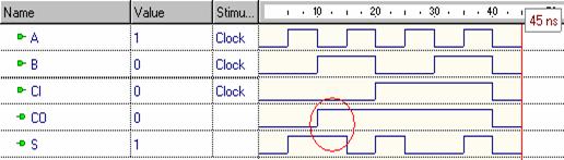
Figure 44
- With the simulation still initialized, we went back to our schematic design by clicking the design’s tab in the main window.
- Then, we restarted the simulation. Since we were using clocks of 10 ns, 20 ns, and 40 ns, we knew that the first problem arose at 10 ns. Therefore, we entered 10 ns in the “Run For” field in the toolbar, and ran the simulation with the schematic open.
- The sum waveform showed that the sum was correct. Therefore, we focused on the carryout logic. When running a simulation, there are boxes next to each input and output signal in the schematic that display their values throughout the simulation. A green box means the signal is low (0), a red box means the signal is high (1), a yellow box (z) means the signal is unconnected, and a blue box (x) means the signal is unknown. We noticed that after running the simulation for 10 ns that the box next to the carryout output terminal was red (see Figure 45 on the next page). Using the mouse-over feature, we traced the signal from the carryout terminal all the way back to the input signals.
- Since
the carryout is determined by the 3-input OR gate, we knew that the
outputs of each of the
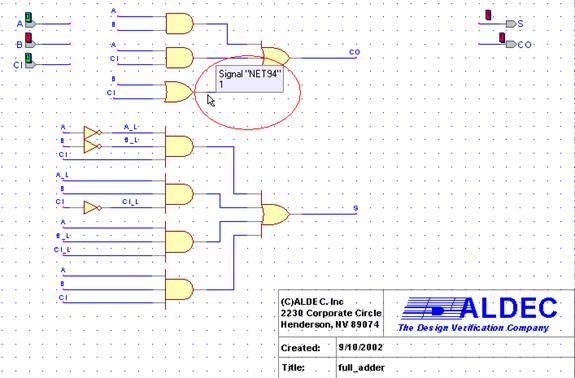
Figure 45
10. Next,
we needed to verify that the inputs were correct. By rolling the mouse over the
two inputs to the OR gate, we verified that the inputs were indeed correct.
Since the signal ‘B’ was a 1 and the signal ‘C’ was a 0, the only way that we
could have produced a 0 for the output was with an
- We
replaced the part by right-clicking it, and selecting the “Replace Symbol”
option and selected a 2-input
This is a simplified example of what you may encounter in
your design process. However, the techniques described above can be applied in
the same way to larger, more complicated designs. You need to know how to debug
your designs using a simulation as well as the
Using Stimulators (other than a clock)
This section will describe two of the available stimulators that you may use in your simulations other than the Clock option you used above.
Value:
The value option allows you to set a value of a signal to 1, 0, z (high impedance), or x (unknown). For this tutorial choose either 1 or 0 by following the steps below.
1. With the Stimulators window open and a signal selected, click the “Value” option in the list.
2. Select the desired value from the “Force value” field (see Figure 46 on the next page).
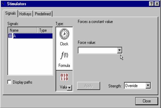
Figure 46
3. Click Apply, and repeat the steps above for other signals. When you are finished, click the Close button.
Formula:
1. With the Stimulators window open and a signal selected, click the “Formula” option in the list.
2. In the “Enter formula” field, enter the value (1 or 0) followed by a space and the time at which to assert this value. For example, the following formula will cause a signal to start out at 1, then change to 0 at 10 us and back to 1 at 20 us: 1 0 us, 0 10 us, 1 20 us (see Figure 47).
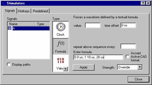
Figure 47
3. Alternatively, you can let Active-HDL create the formula for you by entering the desired value and time offset in the fields provided. You are allowed three sets of these values, then you can choose to repeat the sequence by entering a time in the “repeat above sequence every” field. Once you have set your formula click the Apply button.
4. To set formulas for more signals simply add the signals and repeat the above steps. When you are finished, click the Close button.
Concluding Remarks
This completes the first tutorial for Active-HDL. Remember that this tutorial has only scratched the surface of the capabilities of this program. We strongly recommend you practice using the techniques described within this tutorial while experimenting with and exploring other methods and techniques that Active-HDL offers. You may want to try the Verilog tutorial that comes with Active-HDL as well. Don’t be discouraged if you do not understand what all of the tools are used for or the concepts the tutorial covers that have not yet been covered in class. By spending time with this tool and experimenting, you will save time by being better prepared for the more complicated upcoming assignments.