CSE 370 Introductory Laboratory Assignment
Constructing Simple Logic Circuits - III
Assigned: Monday, October 19, 2009
Due: End of Lab Section
Objectives
In this laboratory assignment you will continue to learn how to use the
Aldec Active-HDL tool. This time the focus will be on how to create Verilog
modules. You will also see how Verilog modules can be used as test
fixtures to help you verify your circuit. By the end of this lab you
should feel comfortable creating a Verilog module directly and setting up a
test fixture.
**Save all the files that you create in this lab. We will use them
later.
Tasks
-
Read Part 1 of Tutorial #2
to familiarize yourself with test fixtures and how to use them to test
a circuit in Active-HDL. You will need to know this for the next task.
-
Complete Tutorial #3 which
descries how to write simple Verilog modules and use them in
schematics. As part of the tutorial, you will write and test the
Verilog module for a full-adder; a full adder is an adder that
handles both carry-in and carry-out conditions in addition to the sums
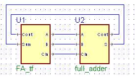
and two inputs. You should create a test schematic by using the
provided test fixture: FA_tf.v (right click
and "save as" if the download doesn’t start automatically). Test
fixtures will be covered in more detail later so don’t worry too much
about why it works. However the basic premise is the test fixture
generates a signal and checks to see if the returned signal is the
expected output. An example of how to hook up your test fixture is
below.
To test to see if your full adder works you do not have to manually
create signals and simulate it in Active-HDL. Since you now have a test
fixture, the test fixture should generate the signals so all you need
to do is run the simulation. The test fixture should pass in a series
of values to your full adder, if all goes well the console at the
bottom will inform you that your full adder passed. If there are errors
it will let you know as well.
**CAUTION: Do put complete faith in test fixtures, you should always
practice common sense and make sure that the values that come out make
sense. If you see a value like: X, that probably is not right.
-
Complete Part 2 of Tutorial #2
, which describes how to use buses and bus inputs and output
terminals. A bus is simply a large group of wires, which means they can
handle more than 1 signal, for example: an 8-bit bus can have 8
different signals across it. In Part 2 you will create a four-bit full
adder by using one-bit full adders you created in Task 2. You can test
your four bit full adder by using this test fixture: addsub4_tf.v.
*Attention: In the tutorial the four-bit full adder is made with the
pink lib370 gates. However, since we will eventually be putting this
four-bit adder on standard industry hardware you should use the built-
in symbols included with Active HDL, these are yellow. If you have any
pink gates, when you get to the lab where you need to put this design
onto the FPGA (Field Programmable Gate Array), it will not work.
-
Create a Block Diagram in Active-HDL to detect a Fibonacci number
between 1 and 15. These numbers would be: 1, 2, 3, 5, 8, 13. Test it
with the provided test fixture here:
fibonacci_tf.v. Once again since you will have to build this on the
circuit board we are giving you a level of leeway in the design of the
module, though it is highly suggested that you use logic that can be
constructed (such as NANDs and NORs) from the chips in your kit. You
can refer to the chip map to recall what
logic gates are available to you. If you would like your TA to check
your boolean logic before moving onto to the last step of building your
circuit on the actual board, feel free to call over a TA.
Don’t cares can be useful when simplifying a circuit. As long as
you are feeling up to it, you may treat 0 as a don’t care, though you
should let your TA know if you have done so when the TA comes to check
off your Fibonacci circuit. And finally, Active-High or Active-Low it
is up to you.
-
Using the logic you created in Active-HDL, follow it and build your
Fibonacci Detector on the circuit board. You will need 4 switches and 1
LED. We suggest that you use SW0 through SW3, where SW3 is the most
significant and SW0 is the least. If you have any trouble with this
last part and your logic is correct, you should check your wiring with
the logic probe. You can use the logic probe to trace through each step
of the circuit and check for unexpected outputs or inputs.
Lab Demonstration/Turn-In Requirements
A TA needs to "Check You Off" for each of the tasks listed below.
-
Demonstrate your working 4-bit full adder design from Task 3.
Do not wire up this circuit with your chips on your board.
-
Demonstrate your working Fibonacci circuit from Task 5.
Do wire up your Fibonacci circuit with your chips on your board.
Comments to:cse370-webmaster@cs.washington.edu