CSE370 PAL Tutorial - Using Active-HDL to Compile to PALs
Programmable Array Logic: Specification, Compilation, and Programming
Objectives
This tutorial will familiarize you with the process of mapping logic to a PAL and programming the PAL so that is ready to include on your protoboard along with other circuitry. In the following, a Verilog file describing a counter is used as an example. However, you'll use a Verilog file of your own to specify the logic to implemented in the PAL. After completing this tutorial you will know how to:
- Specify that a PAL is to be used to implement a block in your design;
- Instruct the tool as to the particular PAL to which the logic will be mapped;
- Run the compilation process and read the resulting reports about how the mapping proceeded including how to read the pin map for the part; and
- Program the PAL so that it is ready to be used on your prototyping board.
Even though this tutorial will show you all you need to know to create basic PALs, you should experiment with Active-HDL on your own. You will find that there are many tools and options that have been left out of this tutorial for the sake of simplicity. By experimenting with these tools on your own, you will become more proficient with Active-HDL, and you may find different methods that better suit your style, while still achieving the same design goals.
Start Active-HDL
- Open Active-HDL.
- Select the “Open
existing work
- Click OK.
* If you have forgotten how to use the “More…” button refer back to a previous tutorial.
Using a PAL in a Design
4. IMPORTANT Before creating a new design, choose Preferences from the Tools menu. (not shown)
5. Under Environment, choose the Default HDL Language to be Verilog.
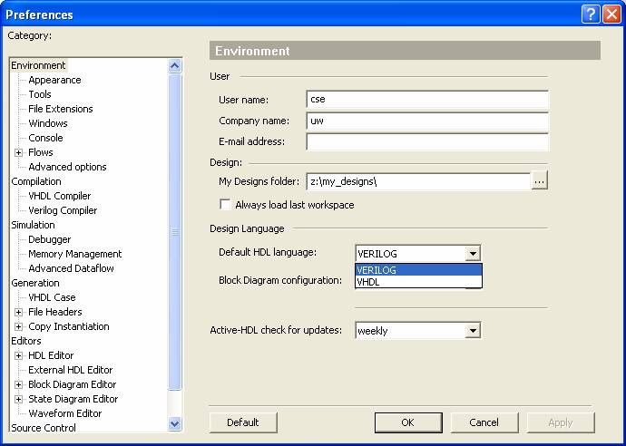
Figure 0
6. Now that we have the default language set to Verilog, we want to create a new design. Select new design from the file menu. (not shown).
7. Choose Create an Empty Design with Design Flow and click next.
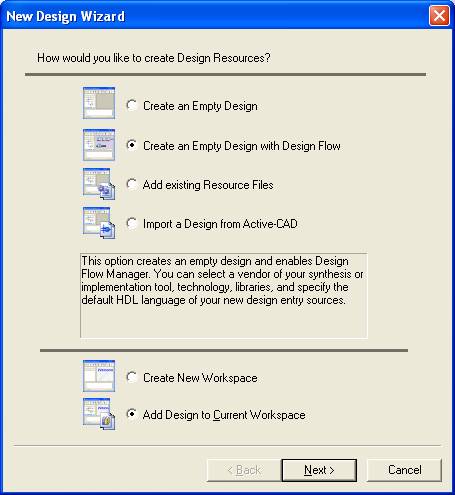
Figure 0.1
8. Click next again. Name your design something like tutorial3. Click next then finish.
9. Select Add New File under your new design. Click the Add Existing File button.
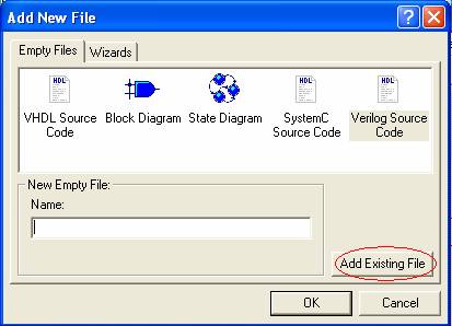
Figure 0.2
10. Select the Verilog file for the full-adder circuit you created in Tutorial 2. Make sure the “Make local Copy” check box is selected. Click Add.
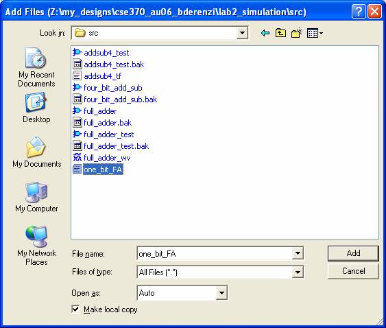
Figure 0.3
11. Compile the verilog source file you just imported.
12. Open the Flow View (if it is not already open) by selecting the View Flows button:
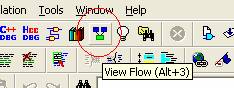
Figure 1
13. On the design flow tab, select the large Flow Settings button:
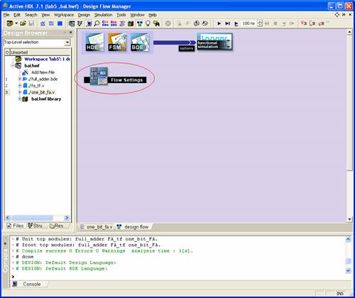
Figure 2
14. Under HDL Synthesis, click the Select button next to the Tool Name text box. (not shown).
15. When the
Select HDL Synthesis Tool dialog appears, expand the
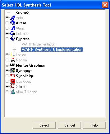
Figure 3
16. Choose OK to return to the design flow screen.
- In the Design Flow page to the left of the “Synthesis & Implementation” icon you will see an options button. Click the options button (Highlighted orange in Figure below).
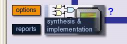
Figure 6
- Ensure that the Top Level
Unit drop down has your Verilog file in it. If not, change it to match the
file you want programmed in the PAL. Note: For a file to be listed in the
Top Level Unit drop down box it must already be compiled. Change the Family
to
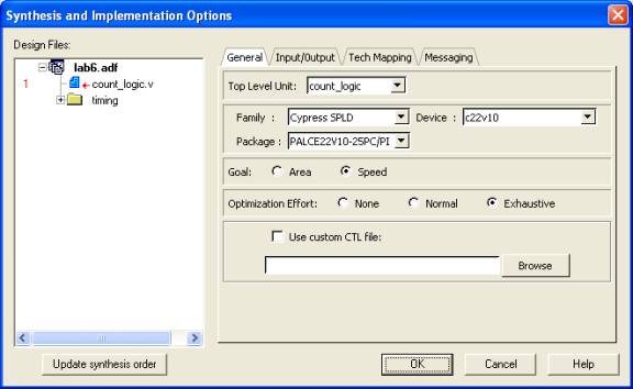
Figure 7 (a different version, but the same)
- When you are ready to generate the files to program your PAL click on the “Synthesis & Implementation” icon (shown in figure below) on the Design Flow page. This will cause a file of type *.jed to be generated that can be used to program your PAL. NOTE: Only click on the synthesis & implementation button once. You will need the log file for the next step to determine the pin configuration. If aldec starts a second synthesis it will clear the log files. When performing a new synthesis, aldec clears the log files in preparation for the new synthesis but then does NOT perform a new synthesis because the old synthesis is up-to-date. This leaves you with a blank log file. If this happens and your log file is blank, change something in your Verilog file, save it, recompile it, then synthesize it. This will cause aldec to perform a new synthesis and generate a new log since the source file changed causing the files to be out-of-date.
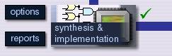
Figure 8
- After the synthesis completes click the reports button that is located to the left of the Synthesis & Implementation button. (Highlighted orange in Figure below).

Figure 9
- You should look at this report carefully and make sure you understand all its parts. Double click on the report for your Verilog module and scroll down until you find the diagram the displays the location of the pins. The diagram should similar to the figure below. NOTE: Pin 12 is GND and Pin 24 is Vcc even though they say not used. You might want to save this part of the log for future reference when you use your PAL on your protoboard. Note that the pins are assigned by the tool. In a later tutorial, we'll learn how to specify where each input and output should be assigned.
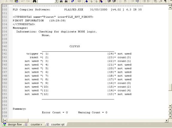
Figure 10
- Goto the special PAL programming station in the lab and logon as the appropriate user that contains your .jed file on its network share.
- Place your 22V10 PAL chip in
the programmer. First lift the release lever so that it is pointing
straight up. The TOP of the chip (end with notch) should be away from the
lever(see diagram on right of programmer). Place the chip in the
programmer so that the chip is as close to the lever as possible. This
means that all the extra
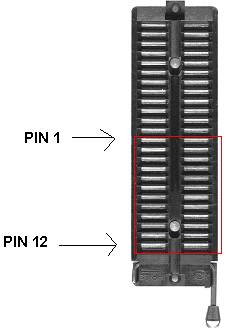
Figure 11
- From the programs menu go to BK PRECISION and open the program PG4uw. After BK PRECISION opens and finds the programmer, verify the programmer is working by looking on the “programmer” box in the bottom of the window under status(red circle in Figure 12) it should say “ready,” if it doesn’t contact the course staff. IMPORTANT: Verify the programmer is setup for your PAL by looking at the “Device” window located at the bottom of the screen(red arrow in Figure 12) and making sure the program lists “Cypress PALCE22V10” as the Device. If the Cypress PALCE22V10 is listed SKIP step #18 and go to step #21. If another device is listed go to step #18.
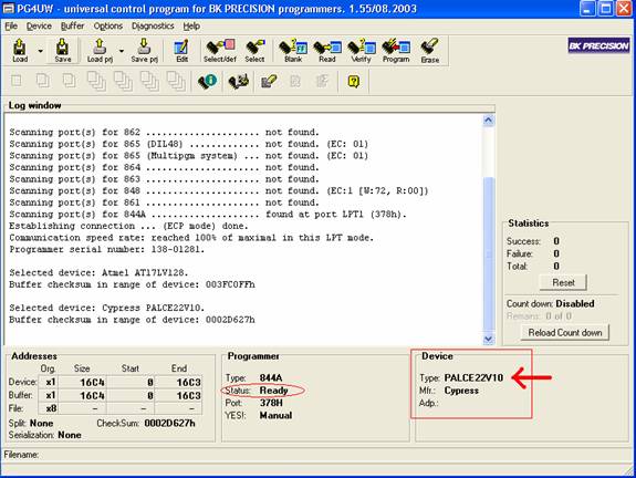
Figure 12
- To setup the programmer to
select your PAL go to the “Device” menu and click on
“Select Device.” In the Select Device window (shown in figure
below) type “Cypress PALCE22V10” in the Search field. There
are several
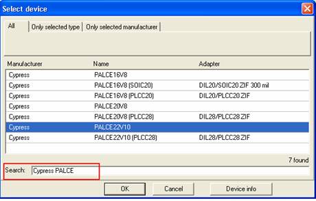
Figure 13
- Next you will need to setup the options you will be able to perform on this chip. Select the menu option “Operation options,” which is located under the “Device” menu and the “Device options” sub menu.
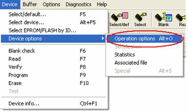
Figure 14
- In the Device Operation Options window make sure the “Device” checkbox has a check in it. Click OK.
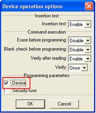
Figure 15
- Select Load from the File menu and navigate to your .jed file and click open.
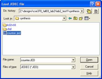
Figure 16
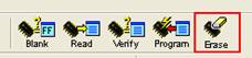
- Click the Erase Button on
the toolbar to erase the PAL
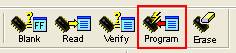
- Click the Program button on
the toolbar to load your .jed file onto the PAL.
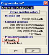
- A window will appear asking for confirmation. Make sure the Device box has a check mar. If the check mark is present click YES. If a check mark does not appear, click no and go to step 5.
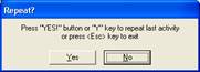
- After the device finishes programming a window will come up and ask if you want to repeat this action. Click on the no button
- Congratulations you have programmed your PAL. Remember to Exit BK PRECISION, remove the PAL from the programmer, and log out of the computer for the next person.
Concluding Remarks
You should now understand how to program a PAL to implement logic you specified in a Verilog file. You should have a sense for the tool flow that compiles a specification, a set of Boolean equations, fits them to a particular device (in this case, the 22V10), and then creates a programming file to match. You should have also learned to use the PAL programmer in the lab and have a PAL ready to use in yoiur protoboard.