CSE 370 Introductory Laboratory Tutorial

Synthesizing onto a FPGA


This tutorial will walk you through the steps of implementing a design made in Active-HDL onto the Altera Cyclone II FPGA. Before we begin, you should locate the design you made in Tutorial 2, it is the same 4 bit adder/subtractor that you implemented previously. The file should be of the format "(name).bde" meaning that it is a block diagram design. You will also need you Full Adder verilog design that you made as well. The file should be of the format "(name).v" meaning that it is a verilog file. The typical location where these files are stored is:


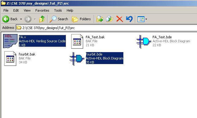
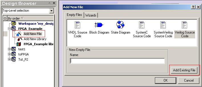
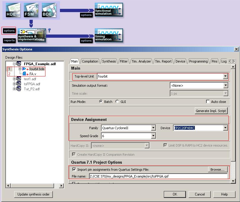
..my_designs\(Design Name)\src\(name).bde
..my_designs\(Design Name)\src\(name).v


Once you have located these two files, open up Active-HDL. Select (File)> (New)>(Design) and choose the option [Create an Empty Design with Design Flow] and make sure that you have [Add Design to Current Workspace] selected as well. When all these settings are set, click [Next>].


You should see a window that allows you set up various settings for your design. First check to make sure that the [Block Diagram Configuration] is set to use (Default HDL Language). You should now click on the [Flow Settings] button so that we can tell Active-HDL what hardware and software we are using. Under the [HDL Synthesis:] you should set the Tool to be (Altera QuartusII Synthesis & Implementation 7.1). Also you need to set the [Family:] to be (Quartus Cyclone II). When all of this is done, click [OK] and then [Next>] to move on.


On this screen, choose an appropriate name for your design. Remember that you should not begin your names with numbers, or other odd characters. Also your names cannot contain spaces to avoid problems with software in the future. Click through the rest of the dialogue boxes until you see that your design has been added to your workspace. The various icons and buttons on the right is the Design Flow. Active HDL uses it to guide you through the process of synthesizing and implementing your design onto the FPGA.


Now that we have created our design we are ready to add the files we need to synthesize the Four Bit Adder/Subtractor onto the FPGA. Double click the [Add New File] underneath your design name and select [Add Existing File] because we already created the design files we are implementing. Navigate to where you stored your Four Bit Adder/Subtractor and your Full Adder verilog file and add them to your design. Make sure that [Make Local Copy] is checked so that you do not modify the original files. Once you have added your files you should see them underneath your design. At this point you should compile these files, make sure that your Four Bit adder compiles with the M next to it as shown in the image. If you see a D, you will have to change the target language by going to (Design)>(Change Target HDL) and select Verilog instead of EDIF and click [OK]. From there you should recompile and the M should appear.

Adding a new file.

Selecting the two files.

After compiling the files.


Check your Four Bit Adder/Subtractor circuit, does it look like the one below? It is important that you are using the yellow symbols and not the pink ones because the pink ones will not synthesize correctly onto the FPGA.


There is one last piece that we need to create before synthesizing onto the FPGA. Since the FPGA doesn’t know what the various Inputs and Outputs in your design are connected to, we have to create a (.qsf) file for the FPGA to read and use. If we don’t create one the FPGA will randomly assign pins to be outputs and inputs and that could be very bad considering the FPGA has hundreds of pins. You can think of the (.qsf) like a settings file which you use to inform the FPGA what pins you want connected to what.

For this lab we want to use the switches, buttons and LEDs for our inputs and outputs. The reason why we need to assign switches, buttons, and LEDs during the synthesis is because the old connections you were using is actually a program that was preloaded into the FPGA redirecting the outputs in and inputs of the Switches, LEDs, and Buttons from their standard inputs and outputs to the connectors on the board. Of course now that everything is on the FPGA, you can’t actually wire a connection from those pinouts into the FPGA, so we have to program in our connections. Luckily for us, the FPGA has pins which are directly connected to the switches, buttons and LEDs. Creating a (.qsf) file is pretty easy, the FPGA follows a very straight forward format. For example, the pin connected to Switch 0 is called [PIN_L22], so to assign one of our inputs to PIN_L22 we use the following:

set_location_assignment PIN_L22 -to A[0]

By using that line of text we have assigned Switch 0 to be the first input of A. If you look at our design above, you will see that there is A[0] through A[3], so each of those will need a pin assigned to it. It’s easy because we can directly reference the names we used in our design. Go ahead and create the (.qsf) file and save it in the [src] folder of your design. Remember to use good naming conventions for your file by avoiding numbers and spaces. You can refer to this file pinouts.html to see what pins are connected to what inputs/outputs on the FPGA. Make sure you don’t miss any of your inputs and outputs, you should have assignments for:

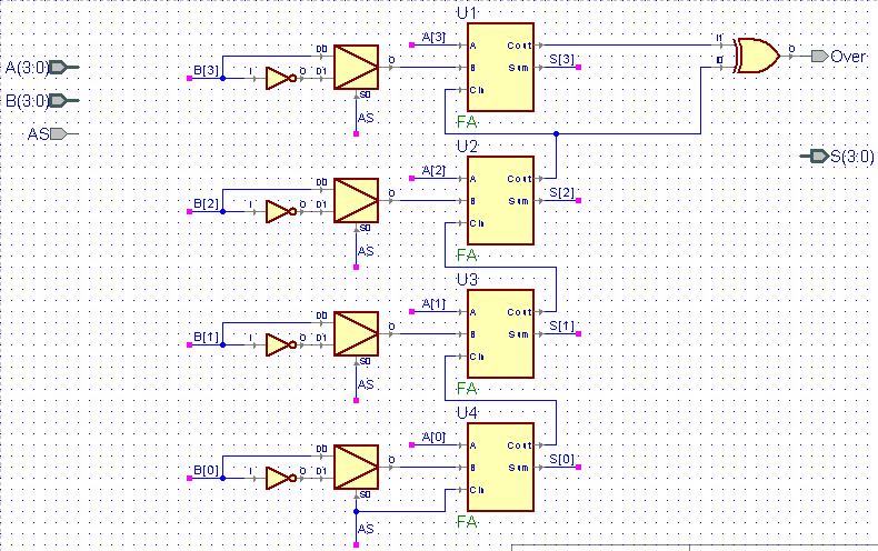
A[0], A[1], A[2], A[3], B[0], B[1], B[2], B[3], AS, Over, S[0], S[1], S[2], S[3]

Now that we have created the final piece needed to synthesize onto the FPGA we can actually begin the actual process of putting the design onto the FPGA. Go back to the Design Flow that we saw earlier. There is a quick button at the top of the screen that you can click that will bring you to the Design Flow as well.


From here you should click on the [options] button next to [synthesis & implementation] to gain access to the window where we will set up our configuration for the FPGA. Once you click on the options button a (Synthesis Options) window will come up. The first thing to check is to make sure all the important files are selected in the (Design Files) browser on the left side of the window. For this design we need to make sure the Four Bit Adder/Subtractor will be included as well as the Full Adder design. You know it’s included when there is a little red arrow next to the file.

Next we need to select the (Top-level Unit), this is the primary design that will be put on the FPGA. Since we are trying to put the Four Bit Adder/Subtractor on the FPGA we will choose that as our (Top-level Unit). If we were only synthesizing the Full Adder, we could choose the Full Adder’s design instead from the drop down menu. The (Simulation output format) should be None and the (Time Scale) should be 1 ps. Make sure the (Run Mode) is set to Batch. Next under Device Assignment we need to tell the program what kind of FPGA we have. The (Family) should be Quartus CycloneII, and the (Device) should be EP2C20F484C, this is the same serial that is written directly on the FPGA chip. You could see it if your breadboard wasn’t covering it. When you change the (Device) the (Speed Grade) should automatically be updated to 6.

Finally the last setting that you need to add in is to set up the pin assignment. Check the little box that says (Imput pin assignment from Quartus Settings File) and Browse to your (.qsf) file that you made and select it. This way the program will use the pinouts that you assigned in the (.qsf) file. Now you are all set. Check to make sure the settings are all right and click [OK].


Now that everything is all set. Click on the [Syntehsis & Implementation] button and let the program do its work. If everything worked well, the Quartus 7.1 window will pop open and do all of the necessary work to create a file that you can program onto the FPGA. There is an odd problem about Active-HDL, it will throw an error even when there are no errors. So if you see red text that says Quartus 7.1 finished with errors, in the Active-HDL console you should ignore it when Quartus itself says it did not have any errors. Take a look at the picture below if you’re confused.

In this case Quartus 7.1 states that it had 0 errors and 0 warnings. This is correct. You should ignore the statement in Active-HDL that says there were Errors and Warnings if Quartus states there were no errors and warnings.

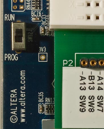
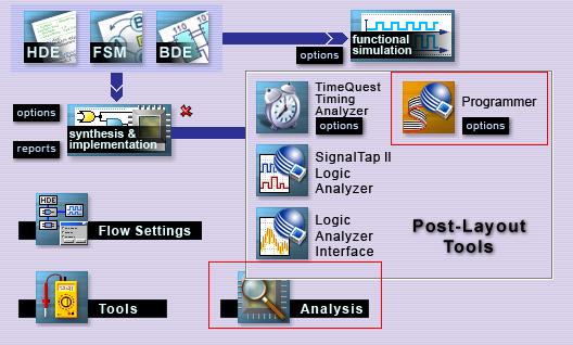
Great, now we have finally made a programming file that we can program onto the FPGA board. Turn on your FPGA board, make sure it runs and is flashing the usual CSE 370 across the HEX display. Check to make sure the USB cord is fastened securely and plugged into the board. Finally check to make sure the little switch below the power button is on the RUN side and not the PROG side. With all of this ready, click on the [Analysis] button on the Design Flow, and then click on the [Programmer] button.


The QuartusII Programmer will pop up. This is the interface that connects your computer to the FPGA via the USB. Check to make sure that the Hardware is set up correctly, you should see that the connection is via (USB- Blaster), if you don’t see this, click on the [Hardware Setup] button and select the connection to be via the USB-Blaster. Make sure that the (Mode) Is in JTAG. Those are the final configuration steps. Now click on the [Add File] button and navigate to your design folder. Under your design folder you should see a folder called: synthesis. Select the (.sof) file, this is the programming file that you will load onto the FPGA and [Open] it.
You have another option which isn't shown in the picture below. When you click on the [Programmer] button under [Analysis] you can click on the little {Options} tag next to the [Programmer] button to select the programming file ahead of time.


Now all that is left is to program the file onto your FPGA. Check the little box under [Program/Configure] and click the [Start] button to program your design onto the FPGA. Test it and see if it worked!


Comments to: cse370- webmaster@cs.washington.edu