CSE370 Laboratory Assignment 5
Case Studies in Combinational Logic
Distributed: April 21, 2006
Due: End of lab session
Objectives
In this laboratory assignment you
will use your combinational logic skills to design and implement
two of the case studies from Chapter 5 of the textbook. You
will create a Telephone Keypad Decoder (pg 227) and a 4-bit
adder/subtractor (pg 239).
Special Notes:
1) This lab contains many details that MUST be correct for the everything to
work so please pay close attention to the instructions. When something is not
working read the instructions a second or third time to make sure
you have completed every step properly. We recommend that you
read all the instructions before starting to implement the circuit to make
sure you understand where you are headed and the special notes you will need
along the way.
2) Unfortunately, the PAL synthesis tools can not currently complete
synthesis and implementation of a circuit if the gates from lib370
are used in the creation of the circuit. The PAL synthesis tools can complete
synthesis and implementation if the circuit is constructed with verilog
code and Active-HDL's built-in symbols/gates. In part 1 of this lab
we will deviate from the normal course policy of using ONLY lib370 gates.
The overall class policy will remain the same so you should always
use lib370 gates with the single exception of PAL synthesis. If you
accidently forget to use lib370 gates on a homework or during
lab you may be asked to redo the assignment or may lose
points. The only time it is acceptable to use Active-HDL's built-in
symbols/gates is when the instructions explicitly tell you to use them for PAL
synthesis.
3) This laboratory assignment has TWO checkoff points instead of the normal
single checkout at the end.
Modules you will use from previous labs:
-
Your verilog implementation of a full adder from Lab #4
Tasks
Part 1 (May be completed before Lab)
-
If you don't already have one, create a 4-bit adder/subtractor as you did in
Part 2 of Active-HDL Tutorial #2.
Remember to use only verilog or the built-in symbols/gates in your circuit so
that it can be synthesized to the PAL in Part 2.(Test Fixture)
-
Read CLD-II Section 5.3 (pages 227-231).
Part
2
-
In Part 2 of the lab you will take your 4-bit adder/subtractor implementation
from Part1 and will wire it up on a prototyping board using a PAL.
-
Create a CTL file to specify which pins the inputs and
outputs of your 4bit adder/subtractor should be assigned to on the PAL
chip. Here is a description of how
to create a CTL file.
-
Synthesize your 4bit adder/subtractor from Part 1 for a PAL. Make sure
you include the correct files (and exclude the others) and
select the correct top level module in the synthesis options before you
synthesize. Also make sure you include your custom CTL file for pin
assignments.
-
You will find that the tools will not be able to implement this circuit to
the PAL since it runs out of product terms. How many product terms does it
need? How many product terms does the 22V10 have? This happens because the
tools try to compile the functions into 2-level circuits, and this
requires way too many product terms.
-
To solve this problem you will need to adjust the synthesis options.
In the Tech Mapping tab of the Options button, change the Node Cost from the
default, which is 10, to 1. This
forces the compiler to be less aggressive about "flattening" your design into a
2-level implementation and, as a result, to keep the ripple-carry adder as the
multi-level circuit that you want. After you complete the synthesis and
implementation of your circuit on to the PAL, test it using
switches for input, and LEDs for output. Unfortunately, there are 9 inputs and
only 8 switches. Use all 4 switches for A's input and 4 switches for B's
input. Use BTN1 as the input to AddSub. NOTE: LED8 is tied directly to SW8
so when you change the value of SW8 when testing, LED8 will also change.
-
Demonstrate your 4-bit adder/subtractor to a TA to receive credit for Part 2.
You should get checked off before moving on to Part 3.
Part
3
NOTE:
There are two types of keypads that will be used in the lab please note the
differences. One keypad is a standard 12 key telephone keypad that
has 8 pins (pins: 1 common pin, 4 row pins, 3 column pins). The second keypad
has 16 keys that include the normal 12 keys on a telephone key pad plus buttons
for A, B, C, and D (pins: 1 common pin, 4 row pins, 4 column pins). Notice the
only difference is that there is an extra column pin for the extra column
of buttons (A, B, C, and D). The keypads should have a black arrow drawn on
them pointing you to the common pin.
-
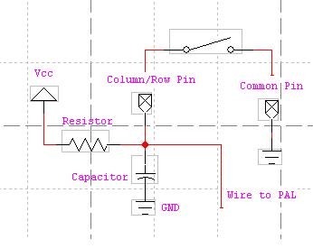
The first step is to wire up the keypad so that you can identify which
pins correspond to which row/column. The diagram below shows how the column/row
buttons should be wired. Please refer to section 5.3 for further details on how
the keypad works. NOTE: The lab's implementation will differ from the
textbook's implementation - in the case of this lab, a button's logic
value will go from HIGH to LOW when pressed. This means you need to
identify which row and column are at a logic LOW to detect which button
was pressed.

Notice the pull up resistor and capacitor that are connected to the Column/Row
pin. These are required for debouncing of the signal from the button. As the
switch is not perfect, it will "bounce" between HIGH and LOW and may fool your
circuit into thinking a button has been pressed multiple times. The
resistor/capacitor provide a way to "slow down" the signal so that the bouncing
doesn't affect it. Read pp. 562-564 of the text for a more detailed description
of the debounding problem and solution.
-
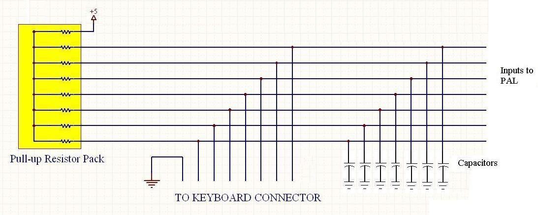
Place the keypad in the breadboard and place a resistor pack in parallel
with the keypads column/row pins so that you connect the
resistor pack to the column/row pins. DO NOT connect the common pin of the
keypad to the resistor pack. Connect the common pin of the keypad to ground.
Connect the pin marked by the dot in the resistor pack to Vcc.
Add the capcitors with one lead of the capictor attached to ground and the
other connected to a column/row pin.

-
Use your logic probe to identify which of the keypad's pins
correspond to which row and/or column so you can wire the PAL to the
appropriate column/row pin.
-
Write a program in verilog to decode which key is being pressed and output a
binary representation of the key pressed. ( 0 through 9, * should correspond to
10, # should correspond to 15). The program should also contain an output that
is true if only one button is pressed and false if multiple buttons have been
pressed. (See section 5.3 in CLD-II) Skeleton Code for
KeypadDecoder
-
Create a CTL file to specify which pins the inputs and
outputs of your telephone keypad decoder should be assigned to on the PAL
chip. Here is a description of how
to create a CTL file.
-
Synthesize your keypad decoder (written in verilog) for the PAL. Make sure
you include the correct files (and exclude the others) and
select the correct top level module in the synthesis options before you
synthesize. Also make sure you include your custom CTL file for pin
assignments.
-
Wire up the inputs of your decoder PAL to the keypad and the outputs to 5 LEDs.
-
Demonstrate your telephone keypad decoder to a TA to receive credit
for Part 3.
Lab Demonstration/Turn-in Requirements:
This lab requires two seperate demonstrations for
"checkoffs"
-
Demonstrate your 4-bit adder/subtractor from Part 2.
-
Demonstrate your telephone keypad decoder from Part 3.
Comments to: mailto:cse370-webmaster@cs

