CSE370 Laboratory Assignment 4
Making a Full Adder with a Multiplexer, Decoder, and PAL
(Programmable Array Logic)
Distributed: April 17, 2006
Due: end of lab period
Objectives
In this laboratory assignment you
will learn to use multiplexers, decoders, and PALs to create a full
adder.
The PAL (Programmable Array Logic) we will be using in this class is
called the 22V10 (here is the functional logic diagram).
This is a very flexible PAL that you will be using in different ways this
quarter. At the core of this PAL are 10 logic blocks that each computes a
Boolean function. This output can either go straight to a pin or through a
register to a pin. We are concerned only with combinational logic right now, so
we will ignore the register. The output also feeds back into the PAL, so that
you can use it to implement multi-level logic functions.
This is how this PAL gets its
name: functions of up to 22 inputs, with 10 distinct outputs, hence,
22V10. Note: for now, ignore the other logic elements in this PAL, we'll
come back to them later in the quarter. After you familiarize yourself
with the component, you will write some Verilog code that will be compiled into
the logic in this PAL. This is yet another useful capability of the ActiveHDL
tool. We'll use the full-adder circuit from the previous
lab assignment as the example. You will then "program" the PAL
and use it on your protoboard.
Modules you will use from previous labs:
-
Your verilog implementation of a full adder from Lab #4
-
The verilog full adder test fixture (FA_tf.v) from
Tutorial # 3 in Lab #3
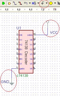
For the Active-HDL schematics in the lab, use only the c74XXX chip packages
in the lib370 library. The following figure shows how to wire in Vcc
and GND signals in Active-HDL.

Tasks
Part 1 (May be completed before Lab)
-
Use a 3:8 decoder (the '138 chip) and gates to implement a full adder with the
c74XX packages in the lib370 library. These chips are identical to the real
chips in your kit. Remember to use
de Morgan's law to pick the right packages. Create
a test circuit schematic using the test fixture given in the
tutorial to test your design. As you design your circuit, be sure to
use the chip maps
as a guide, and pay close attention to the "enable" semantics on the decoder
chip. Print your decoder block diagram for turn-in. (NOTE: You do not
need to hand in your testing block diagram)
-
You can also implement a full-adder using multiplexers. Use
one standard 4:1 multiplexer ('153) for each output (sum and carry-out), along
with inverters as necessary, to implement a full-adder. Note that the '153 chip
actually contains two independent multiplexers, so you only need one of these
chips total. Do not use the 'mux4' part in lib370; use 'c74153.' Create
a test circuit schematic withe the full adder test ficture to verify your
design. Again, pay attention to the enable semantics for the '153.
Print your multiplexor block diagram for turn in. (NOTE:
You do not need to hand in your testing block diagram)
-
Spend some time familiarizing yourself with the 22V10 functional
logic diagram. Make sure you see how logic functions are computed
in this component.
Part 2
-
Complete the entire PAL tutorial
that explains how to compile a circuit into a PAL using ActiveHDL and the
Cypress compiler. Now compile your full-adder Verilog module (from the
previous lab) and then program it into a PAL using the PAL
"programmer". You should already have the Verilog file for this circuit
and have verified it using the simulator. The PAL is the long chip with
the image of a tree on it, and you should already have 2-3 of them in your kit.
-
After you've programmed your PAL, place it in your circuit board and wire its
inputs and outputs to some switches and LEDs, respectively. Use SW1 for A,
SW2 for B, and SW3 for Cin and LED1 for the Sum and LED2 for the Cout.
Verify that the full adder operates correctly. Make
sure you leave room for the multiplexer and decoder chips on the
breadboard. In addition, you should make sure to review the reports
generated by the compilation process and understand what equations were
generated to be implemented by the PAL. The TAs may ask you about
this, so be sure to review it carefully.
-
Wire up your multiplexor implementation of your full adder using the
same switches for A, B and Cout as the PAL but use LED3 for the Sum and
LED4 for the Cout.
-
Demonstrate the two implementations of a full adder to a TA.
Lab Demonstration/Turn-in Requirements:
A TA will "check you off" after you:
-
Hand in a print out of your decoder implementation using c74XXX gates in
Active-HDL.
-
Hand in a print out of your multiplexer implementation using c74XXX gates in
Active-HDL.
-
Demonstrate both the PAL and multiplexer implementations on your prototyping
board.
Comments to: mailto:cse370-webmaster@cs
