CSE370 Introductory Laboratory Assignment
Constructing Simple Logic Circuits
Distributed: Monday, March 27, 2006
Due: By the end of the lab session
Objectives
This first laboratory assignment will help you get familiar with the
prototyping board and Aldec's Active-HDL both of which you will be using
the entire quarter. We will be using Aldec's Active-HDL as our primary
design tool this quarter. In this laboratory assignment, you will learn how to
use the tool to create and simulate basic schematic diagrams. In the
future we will expect you to use this tool to do part of your written
assignments. The goal of this lab is to introduce you to 1)
Active-HDL's schematic editor and simulator and 2) the prototyping board you
will be using in lab.
Each student should complete this lab individually.
We also hope that you will become familiar with us, your TAs, this means ask us
questions. We always encourage you to ask questions and there is no such
thing as a stupid question, especially for this first lab. For many of
you, this may be the first time you've ever touched a wire, so if you unsure of
ANYTHING, please ask us.
Tasks
-
Complete the entire introductory tutorial
to Aldec's Active-HDL 6.2. By the end of the tutorial you should have
placed an AND and OR gate in a schematic from the lib370 part library
and simulated this circuit for all possible input values. Hand in the
printout of your simulation output.
-
Construct and verify the operation of a small circuit (1-2 logic gates) using
switches and LEDs as I/O devices.
Laboratory Design Kits
The design kits contain everything that
you need to construct and test medium size circuits. You will be expected to
return the kit in good condition and with everything intact, including the
chips. Included in the DesignKit are:
-
-
Power supply
-
Logic probe
-
Bag of pre-cut, pre-stripped wires
-
Wire stripper/cutter
-
Needle-nose pliers
-
-
Chip extractor tool (the only way you will remove
chips from the breadboard - for the safety of your fingers and the chip's pins)
Please make sure that all of the above are
in your kit. We may provide additional materials later in the quarter
that you will need for the later labs and the lab project, such as a serial
cable, an LCD display or a keypad.
Accidents do happen, so we will replace a certain number of
chips whose pins may get bent. Generally, the first time,
most any damage will be forgiven. However, incidents of gross negligence will
not be met with such forgiveness. You may be expected to
pay replacement costs for incidents of gross negligence. In particular, you
should pay careful attention to the location of your power wires and never allow a
short between them and ground (GND- 0 volts, and VDD- 5 volts). And please make sure to treat the prototyping
board with care; in particular, be sure to not break off wires in the connectors.
XLA5 Prototyping Board

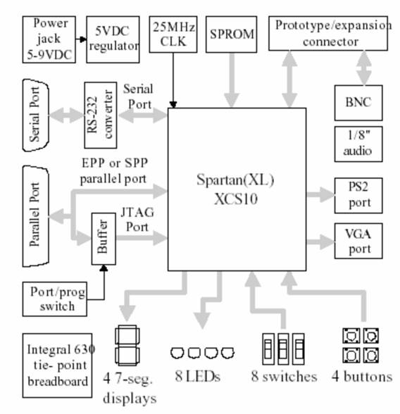
This is a block diagram for the entire XLA board. Note
that it highlights a large programmable logic chip on the board. Your kit
may or may not have this chip in place right now, but we will use it later in
the quarter to provide an environment for your digital circuits. In this
class, you will not program this chip; that will happen in CSE 467. For
now, your focus will be on the upper right hand corner - the prototyping
area. You will also make use of buttons, switches, LEDs, and 7-segment
displays as I/O devices
except for Switch 8, Pushbutton 4, and LED 8, which are used
for special functions. For the final
laboratory assignment, we may make use of other features on the board.
Breadboarding Techniques
The breadboard
on the XLA board is the large white plastic area in the center of the board and
is comprised of 63 rows (numbered 1-63) and 10 columns (lettered a-j) of
holes. On every row, holes in columns a, b, c, d, and e are connected
together underneath the white plastic. So are the holes in columns f, g,
h, i, and j. There are no connections across rows so that all the holes
in row 1 are in no way connected to any of the holes in row 2 and so on.
Therefore you can think of the prototyping area as providing 126 (63 rows split
in half by the trough) 5-way connectors for wires. You'll make
connections between these 126 regions using the wires in the bag in your
kit. These should be inserted as perpendicular as possible to the
breadboard and should slide in and out with just a little force. If you
find that there is a lot of resistance in either direction, first review the
wiring guidelines below, and if that doesn't work, then please call over
the TA or one of the lab staff.
Do not try to
force anything larger than stripped wires into the holes, because this could
damage the protoboard (at great cost). If you need more wire help yourself
to the provided spools of uncut wire in the back of lab.
Before doing any work on the protoboard such as
wiring and inserting/removing chips, be sure the power is OFF.
That is, unplug the power connector while you are constructing the
circuit. After you have finished wiring up your design and before you
turn on the power, double check the power and ground connections.
Wiring Guidelines
Wiring your circuit together can often feel
tedious, especially in the beginning. However, if you are patient and
wire your circuit nicely, you will find that you will spend a lot less time
tracking down wiring errors. To aid you in this, here are a few tips to
consider while wiring up your circuit. If anything is unclear, ask your
TA for an example.
-
Make sure your wires are stripped nicely.
This means that when you put the wire in your bread board, there shouldn't be
any un-insulated wire visible and the wire shouldn't crunch against the bottom
of the board.
-
Your wires should always be nice and straight,
there should be no twists or kinks in it, as they can cause your board to short
out when you insert them in your bread board.
-
Arrange the IC chips on the protoboard so
that only short wire connections are needed. Put tightly connected chips
closer together.
-
Try to avoid a jungle of wires. Long
looping wires that go way into the air are easy to pull out (a hard bug to find
later when the circuit doesn't work as intended).
-
Try to maintain a low wiring profile so
that you can reach the pins of the chips and so the chips can be replaced if
necessary. The best connections are those that lie flat on the board.
For those of you that learn better by seeing, here
is a good wiring example and a
bad wiring example.
Using the Logic Probe
The logic probe
provides a very convenient way to check the value of any signal in your
circuit. The probe has two lights, HI and LO, which indicate the value of
the signal. The logic probe responds to the input voltage in two ways
depending on whether CMOS or TTL is selected. We will use the TTL setting
which lights the LO light for voltages <0.8v. and lights the HI light for
voltages >2.3v. If neither light is lit, then the signal is floating
(i.e. not being driven by any active output) or has some value between 0.8 and
2.3v.
Tasks
-
Use your logic probe to determine in which position the switches provide a 0 or
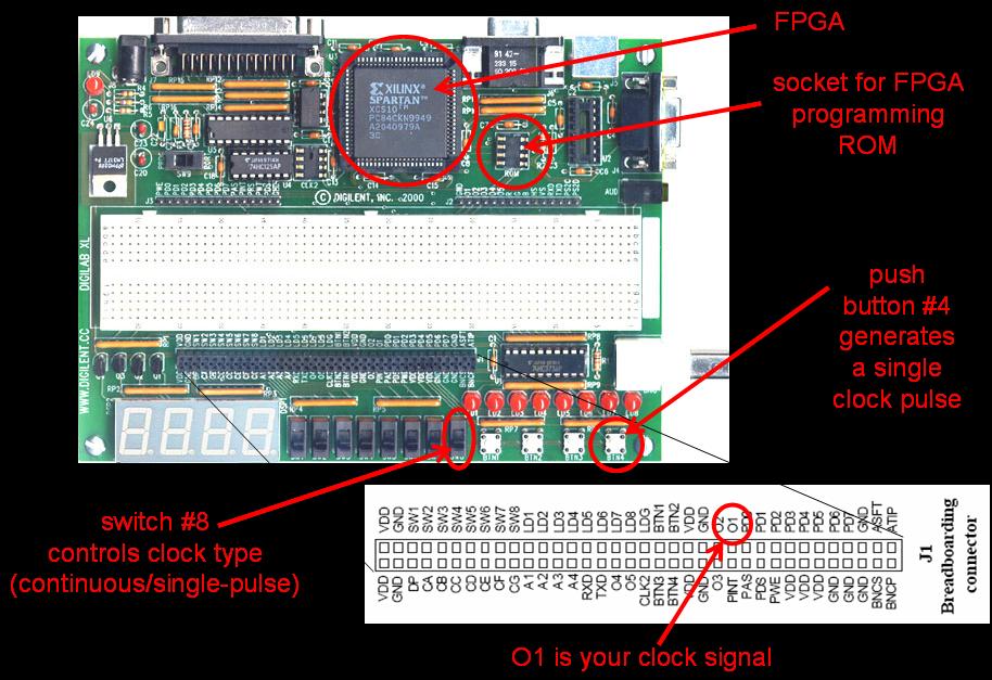
1. Instructions for logic probe usage follow this diagram of your
board and its connectors.
Note that items circled in red, including Switch 8, Pushbutton 4, and LED 8,
have special functions, and should not be used in this lab.

The large black bar just below the white breadboard area is connected to many
of the devices on the XLA board. Connect a wire from the VDD pin in this
black bar to a 5-hole block on the breadboard, and connect another wire from
GND to a different 5-hole block. Place another wire in each of the new
VDD and GND blocks on the board, and leave the other end of the wires dangling. Make
sure they are far apart and don't ever touch, because this will short the power
supply and could cause some smoke or bad odor as parts start to burn (should
this happen, pull out the power cord immediately). Clip the
logic probe's two leads to VDD and GND. The red clip must be connected to VDD
and the black to GND. This is an important color convention to
follow. You have now successfully prepared your logic probe for use.
For now, we will simply use the logic probe to determine which switch positions
correspond to digital high and low signals. Connect a wire from one of the
switches in the black connector bar to a 5-hole block on the breadboard. Remember,
SW8 is already in use, so do not use this switch. You can now
connect power to the board. Now, use the logic probe to "probe" the signal
output by your switch; just (gently) press the tip of the probe in the same
5-hole block as the wire from your switch. You should see either the
probe's red or green light activate. Flip the switch and note that the
light should change as well. Note which switch position corresponds to
"high."
-
Connect a switch to an LED.
Pull out the board's power connection before changing anything -- safety first.
We won't
repeat this again, but you should always remove power before making any wiring
changes and only reconnect it after you've double-checked that you've
wired things correctly.
You can connect the switch and LED directly by just placing a wire between SW1
and LD1 on the black connector. Alternatively, you could use wires to
create connection points in the breadboard area. Reconnect power and
verify that the LED follows the switch.
-
Place an inverter (NOT gate) between the switch and LED.
Now, we'll place our first logic circuit onto the board. Insert a '04
inverter package into an empty region straddling the trough on the
breadboard. Each pin of the chip is now connected to a 5-hole connection
block on the breadboard. Connect wires from the GND and VDD pins of the
'04 to the ground and power connection blocks you set up for part 1. Make
sure to get the right pins: GND is pin 7, and VDD is pin 14 on the '04.
Use the chip maps to ensure you are doing the right
thing and to choose a particular inverter of the 6 on this chip. Connect
the input of the inverter to SW1 and its output to LD1. Now the LED
should light up when the switch is in the opposite position of part 3.
Connect the output of your inverter into a second inverter's input and connect
LD1 to this second inverter's output. We are now back to where we were
before. As one would expect, two inverters logically cancel.
-
Connect a two-input NOR gate to two switches and one LED.
Move the switches to all four possible position combinations and verify that
the NOR gates works as you expected.
Lab
Demonstration/Turn-in Requirements: A TA will "check you off"
after you
-
Demonstrate the NOT and NOR gate working
-
Hand in the printout of your simulation output of the AND and OR gates from
Active-HDL.
Comments to: cse370-webmaster@cs.washington.edu
