CSE370 Laboratory Assignment 5
Introduction to PALs
Distributed: April 20
Due: By the end of lab session (4/25, 26)
Objectives
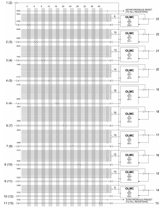
In this laboratory assignment you will learn to use PALs to implement logic functions. The PAL we will be using in this class is called the 22V10 (here is the functional logic diagram). This is a very flexible PAL that you will be using in different ways this quarter. At the core of this PAL are 10 logic blocks that each computes a Boolean function. This output can either go straight to a pin or through a register to a pin. We are concerned only with combinational logic right now, so we will ignore the register. The output also feeds back into the PAL, so that you can use it to implement multi-level logic functions.
This PAL is called a 22V10 because it can implement up to 10 functions of up to 22 inputs. Note: for now, ignore the other logic elements in this PAL, we'll come back to them later in the quarter. After you familiarize yourself with the component, you will write some Verilog code that will be compiled into the logic in this PAL. This is yet another useful capability of the ActiveHDL tool. We'll use the full-adder circuit from the previous lab assignment as the example. You will then “program” the PAL and use it on your protoboard.
Before
you come to lab, complete the Aldec
Tutorial #3, which describes how to write simple Verilog modules and use
them in schematics. You should be able to create the Verilog files and
schematics for steps 1 and 4 of Part 1.
You should also look at the problem in Part 2 and understand how to
solve it.
Part 1
1. As part of the tutorial, you will have written and tested the Verilog module for a full-adder. Create a test schematic and using the test fixture from Lab 3, make sure that your Verilog module works correctly.
2. Spend some time familiarizing yourself with the 22V10 functional logic diagram. Make sure you see how logic functions are computed in this component.
3. Complete the entire PAL tutorial that explains how to compile a circuit into a PAL using ActiveHDL and the Cypress compiler. Now compile your full-adder Verilog module and then program it into a PAL using the PAL programmer”. You should already have the Verilog file for this circuit and have verified it using the simulator. The PAL is the long chip with the image of a tree on it, and you should already have 2-3 of them in your kit. (You will not actually plug the PAL and use it in a circuit until Part 2 of the lab.)
4. Now create a 4-bit adder using your Verilog full adder, and compile it for your PAL using Active-HDL. You can do this by placing 4 full adders in a schematic to create a 4-bit adder. Make sure you label the wires for the carries between the full adders, e.g. with C0, C1, C2. After simulating to prove that it is correct, compile the program for the PAL. Make sure you select the right files and top level module in the synthesis options before you synthesize.
5. You will find that the tools will not be able to compile this circuit to the PAL since it runs out of product terms. How many product terms does it need? How many product terms does the 22V10 have? This happens because the tools try to compile the functions into 2-level circuits, and this requires way too many product terms.
6. To solve this problem, you will have to adjust the compiler options. In the Tech Mapping tab of the Options menu, change the Node Cost from the default, which is 10, to 1. This forces the compiler to be less aggressive about “flattening” your design into a 2-level implementation and, as a result, to keep the ripple-carry adder as the multi-level circuit that you want.
Part 2
Now that you
know how to program a circuit into a PAL, you will now use a PAL to implement a
circuit that converts the output of a keypad into a binary number. This problem
is presented in Section 5.3 of the textbook.
NOTE, however, that for this lab, the keypad outputs are LOW (0) when a
button is pressed, not HIGH as described in the book. Thus you need to figure out which row and
column wires are 0.
NOTE: There are two types of keypads that will be used in the lab so please note the differences. One keypad is a standard 12 key telephone keypad that has 8 pins (pins: 1 common pin, 4 row pins, 3 column pins). The second keypad has 16 keys that include the normal 12 keys on a telephone key pad plus buttons for A, B, C, and D (pins: 1 common pin, 4 row pins, 4 column pins). Notice the only difference is that there is an extra column pin for the extra column of buttons (A, B, C, and D), which we will ignore. The keypads should have a black arrow drawn on them pointing you to the common pin.
1. The diagram below shows how each of the column/row buttons should be wired. Please refer to section 5.3 for further details on how the keypad works.

Notice the pull up resistor and capacitor that are connected to the Column/Row pin. These are required for debouncing the signal from the button. As the switch is not perfect, it will "bounce" between HIGH and LOW and may fool your circuit into thinking a button has been pressed multiple times. The resistor/capacitor provides a way to "slow down" the signal so that the bouncing doesn't affect it. Read pp. 562-564 of the text for a more detailed description of the debouncing problem and solution.
2. Now
you are ready to wire up the keypad and connect it to the PAL. Place the keypad in the breadboard and place
a resistor pack in parallel with the keypad’s column/row
pins so that the resistor pack pins are connected to the column/row pins. DO
NOT connect the common pin of the keypad to the resistor pack. Connect the
common pin of the keypad to ground. Connect one of the unused
pins in the resistor pack to Vcc. Add the capacitors with one lead of the
capacitor attached to ground and the other connected to a column/row pin.

3. Use your logic probe to identify which of the keypad's pins correspond to which row and/or column so you can wire the PAL to the appropriate column/row pin.
4. Now design a circuit that outputs a binary number that indicates which key that is pressed. You will first “program” your circuit by hand for the PAL by drawing X’s on a printout of the 22V10.bmp 22V10.ppt. Use keys 0 through 9 plus * should output 10 and # should output 15. Use an extra output that is set to one when one button is pressed and false if no button or multiple buttons have been pressed.
5. Next write a Verilog program for this circuit. (See section 5.3 in CLD-II) Skeleton Code for KeypadDecoder
6. Create a CTL file to specify which pins the inputs and outputs of your telephone keypad decoder should be assigned to on the PAL chip. Here is a description of how to create a CTL file.
7. Synthesize your keypad decoder Verilog program for the PAL. Make sure you include the correct files (and exclude the others) and select the correct top level module in the synthesis options before you synthesize. Also make sure you include your custom CTL file for pin assignments.
8. Wire up the inputs of your decoder PAL to the keypad and the outputs to 5 LEDs. Verify that is operates correctly and demonstrate it to the TA. In addition, you should make sure to review the reports generated by the compilation process and understand what equations were generated to be implemented by the PAL. The TAs may ask you about this, so be sure to review it carefully.
Hand In
1. The schematic and compilation report for the 4-bit adder from Part 1.
2. Your hand-drawn implementation of the decoder circuit on the 22V10 printout.
3. The Verilog program and compilation report for the keypad decoder, checked off by the TA.
Optional