CS 370
– Spring 2005
Introduction to Digital
Design
Instructor:
Homework Set 6
DISTRIBUTED: May 6
DUE: May 13, Start of class
Collaboration Policy:
Unless otherwise noted, you may collaborate with other CSE370 students on the homework
assignments. Do not look at homework or exam solutions from previous years. You
must spend at least 15 minutes working on a problem before seeking assistance.
Collaboration means that you may discuss the problems and make notes during the
discussion, but you may not look at other student’s work when writing up
your homework. Your homework represents your own work—the homework must
show that you understand the material and have worked as an individual on every
problem. You may not divide up the task of doing the problem sets in the
interpretation of collaboration. You may discuss lecture material with anyone.
Late Homework Policy:
The weekly assignments are due at the beginning of class. Assignments handed in
during or immediately after class will incur a 10% penalty.
We will penalize your assignment 10% per day for each additional day late.
Please show all of your work. Your solutions
must be legible…we will not spend time trying to decipher poorly written
assignments.
The Solution to problem 3 has been passed out in class.
The test fixtures for this homework are linked here and are in the course hw6 folder.
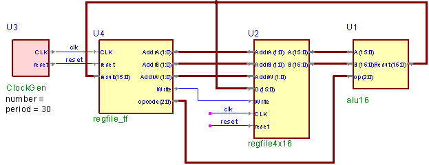
In this assignment, you will continue the design of components for a simple processor. In this assignment you will add a register file to the ALU you’ve already designed.
1. (100 points) You have already designed the most complex component of your processor, the ALU. When the ALU performs an operation, it needs two values for input and a place to store the output. These values will be saved in the registers in what is called a register file. Our register file contains four 16-bit registers numbered 0 to 3. The ALU reads the values from two of these registers and the result is written back to a third. This register file is shown in the figure below labeled regfile4x16. The two addresses AddrA and AddrB indicate which register values are read to the A and B outputs, and AddrW indicates which register is to be written from the D input. This register is written, at the clock edge, only if the Write input signal is asserted. The synchronous reset signal clears the registers in the register file to 0.
Design and test this register file using Active-HDL. Do not use Verilog for this design. The test fixture tests your register file and ALU working together as shown below. On each clock cycle, it specifies an op-code for the ALU and three register addresses for the register file and then makes sure that the result from the ALU is correct. You must change the clock period of the ClockGen to 30ns to give the circuit enough time. To do this, right-click on ClockGen, choose the Properties option and set the actual value of the parameter called "period" to 30. (You have to recompile of course.)
To implement this register file, you will need to make 16 copies of
components like registers. You can do this by actually making 16 copies using
cut-and-paste. (Make the lower bit first with all the signals connected, then
copy the whole thing.) Or you can use the ARRAY feature. Right
click on the component you want to “stack”, and enter the number of
copies you need. Turn on the ARRAY text parameter so you know you've made
an array of 16 copies.
WARNING: Don't use ARRAYs inside of ARRAYs
- there's a bug in the simulator that causes errors sometimes if you do
this. Also, use only simple arrays
– it’s easy to get confused if you try to push the idea too far.
If you are worried about your ALU, we will put a solution in the lib370 folder sometime next week.
2. (20 points) The test fixture for the register file executes “instructions” which tell the ALU what operation to perform and which registers to use for the inputs and output of the operation. Single-step your test fixture (set the simulation time to 30ns., that is, the clock period), and write down what is executed by the test fixture for the first 10 clock periods. You should make a table that looks as follows. Show the values of the registers during the step, not after the result is written back to the register file.
|
Step |
reset |
R0 |
R1 |
R2 |
R3 |
Op code |
AddrA |
A |
AddrB |
B |
AddrW |
Result |
Write |
|
0 |
|
|
|
|
|
|
|
|
|
|
|
|
|
|
1 |
|
|
|
|
|
|
|
|
|
|
|
|
|
|
2 |
|
|
|
|
|
|
|
|
|
|
|
|
|
|
3 |
|
|
|
|
|
|
|
|
|
|
|
|
|
3. (50 points) Design the following circuit that implements the controller for a laser range-finder. The range-finder works as follows: When the start button is pressed, a counter is reset and a laser pulse (ping) is emitted. The counter is then enabled until an echo is detected, at which time the counter is stopped. The value of the counter represents the distance.
Your control circuit has the following inputs:
clk,
reset
start -
Asserted when the start button is pressed.
echo -
Asserted when an echo is detected
and the following outputs:
clearCount -
Assert to clear the counter
enableCount - Assert to enable the
counter
ping -
Cause a laser pulse to be emitted.
Assert for one clock cycle.
a) Draw the state diagram for this controller.
b) Convert the state diagram to a state table.
c) Decide on a state assignment.
d) Synthesize the next state and output logic functions.
e) Draw the final circuit for this FSM. Just include the counter as a component.