CSE370 Laboratory Assignment 9
Final Project : Magnetic Stripe Reader
Part 1 - LCD Interface
Distributed: Monday, November 28, 2005
Due: By the
end
of the next lab session (December 6/7)
Objectives
The final lab project will be designing an interface between a magnetic card stripe reader and an LCD (liquid crystal display). You will work with a partner for the final project which is separated into two parts. In this first part, you will design a simple LCD controller using three 22V10 PALs and behavioral Verilog. In the second part (next week) you will add the interface to magnetic card stripe reader. You will complete the first part by next week, and complete the entire project by the end of the final lab section (December 13/14)
You are now familiar with two very powerful tools: ActiveHDL
and behavioral Verilog, and you will employ them both extensively in order to
complete this assignment. You are also familiar with the design process where
you fully design and simulate a circuit before you try to construct it.
This lab assignment is definitely more challenging than the previous ones, and
you may not be able to finish within the first lab session. However, you will
have an extra week this time to complete the assignment.
Overview
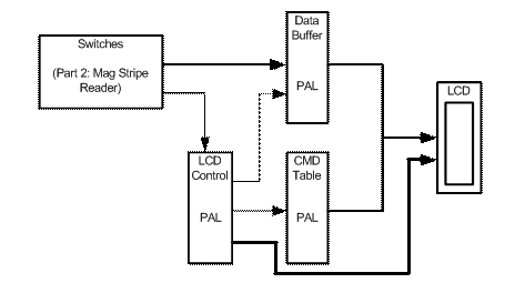
Your goal is to design a circuit which can write an arbitrary ASCII character code entered on your prototyping switches to an LCD display. (In the next lab, characters will be come from the magnetic card stripe reader.) Three PALs will be required to implement this interface: a data buffer, an LCD command "table" and a main control PAL that directs them.
As you can see in the figure below, both commands and data are sent to the display. The commands are used to initialize the display and tell it what to do, and the data is the character to be displayed. The control PAL is the brains behind this outfit. It must first send commands to the display to initialize it, and then send data to the display when it becomes available. Note that the multiplexor that chooses between data from the data buffer and commands from the command table is missing. Instead we will use tri-state buffers in the PALs to implement the multiplexor function.
Only the main controller is sequential. The data buffer and command table are very simple and merely implement combinational logic.

The LCD
The LCD which you will be using has many advanced functions (see the datasheet for a complete explanation), but you will only be concerned with the following two:
- Reset and clear the display.
- Write a character to the display.
The pin layout of the LCD follows:
|
Pin |
Name |
Function |
|
1 |
GND |
0 V |
|
2 |
Vdd |
5 V |
|
3 |
Vo |
1 V |
|
4 |
RS |
High: Data input Low: Instruction input |
|
5 |
R/W |
High: Read from LCD Low: Write to LCD |
|
6 |
E |
Enable the LCD |
|
7 |
DB0 |
Data bus |
|
8 |
DB1 |
|
|
9 |
DB2 |
|
|
10 |
DB3 |
|
|
11 |
DB4 |
|
|
12 |
DB5 |
|
|
13 |
DB6 |
|
|
14 |
DB7 |
Pins 1-3 are power supply connections and will be explained later. Pins 4-14 are signals that you must supply. R/W specifies whether you are reading or writing the display: Since you will only be writing to the display, the R/W signal will always be 0. RS is used to determine whether you are sending a command or ASCII data to the display. E (enable) is used to provide a strobe that causes the operation to be executed. The enable, E, for the LCD is a signal that you must generate: the LCD commits a new character or command on the negative edge of E (something to think about: how do you give E a negative edge?). The data pins contain either an ASCII character code or a command code depending upon the value of RS. You will need to multiplex this data bus between an instruction source and a data source using tri-state drivers in the PAL.
The following is a table with the codes for the 5 commands that you need to execute for this assignment. The first four should be executed in sequence once after reset has been pushed. The last command is used to write a character to the display. You can look at the documentation if you would like to try out other commands.
|
Operation |
RS |
DB[7:0] |
|
Clear Display |
0 |
0000 0001 |
|
Function Set |
0 |
0011 0011 |
|
Display On |
0 |
0000 1100 |
|
Entry Mode Set |
0 |
0000 0110 |
|
Write Character |
1 |
DDDD DDDD |
Your "main controller" PAL will contain a finite state machine that (a) sends the four command sequence to the LCD on reset, and (b) writes characters to the LCD when the input "write" is asserted indicating that a new character is available. This controller FSM will sequence through the commands, asserting the appropriate command or data on the data bus and generating the enable E and RS signals. It will be immediately apparent that one PAL is too small for this. The data bus and control signals E and RS are 10 outputs just by themselves. Thus you will need partition the state machine so that the 8-bit command value is generated by a 2nd PAL that is controlled by the FSM. This "command table" PAL will expand a tightly encoded command code from your main controller into the 8-bit wide command code that the LCD expects. The controller PAL must also control the multiplexing of the command and data onto the databus. We will do this using tri-state drivers: either the command PAL will drive the databus, or the 3rd "data" PAL will drive the databus.
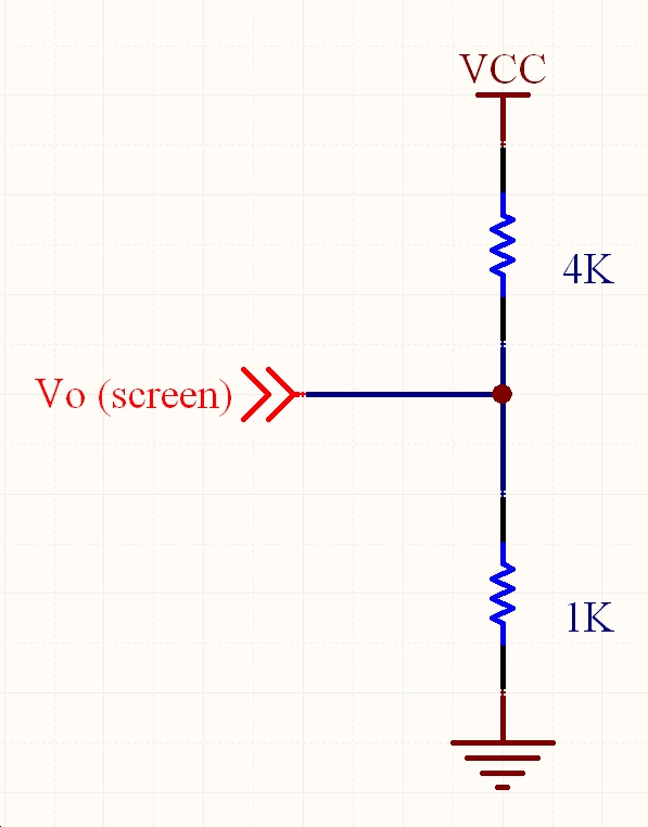
Finally, you will need to set the contrast for the LCD screen. For this, we have to apply a specific voltage at the Vo pin. We can do so with the voltage divider circuit shown in the figure below. It will generate a voltage Vo of approximately 1/(1+4) of Vdd or 20% of 5V (1V). In your kit should be a 3.9K ohm resistor and a 1K ohm resistor (If there aren't any in your kit, they are also on the conference table). You can determine the resistance value of a resistor by the color coded bands on the resistor (see explanation of how the color coded system works).

8-bit Tri-State Driver for the Data Buffer
The following Verilog implements an 8-bit tri-state driver which will serve your purposes for this assignment. You are encouraged to use an intuitive pin assignment. The provided file tri_driver.ctl will do just fine. Note how "turning off" the output of a pin is expressed in Verilog: rather than assigning 0 or 1 to the output, we assign a z, which stands for "not driven". This distinction between no voltage and some voltage is key to understanding this concept. Make sure you understand what each of the three possible states of the output means before moving on with the lab (your output is either (a) off, no voltage, (b) on and a voltage representing a 0, and (c) on and a voltage representing a 1).
module
tri_driver (en, from, to);
input en;
input [7:0] from;
output [7:0] to;
assign to = (en) ? from : 8'bzzzzzzzz;
endmodule
Command Table
The following is a do-nothing stub which you will need to complete for the command table. Again, a sane pin assignment is highly recommended (use lcd_cmd.ctl). Remember that, since you will wire the outputs of the 8-bit tri-state driver together with the outputs of this PAL, you will need to be able to also "turn off" this chip's output when data is being driven to the databus (think z's).
module
lcd_cmd (RS, cmdIndex, lcdCMD);
input
RS;
// Used to tristate the LCD CMD
input [1:0] cmdIndex; // Index of the command
output [7:0] lcdCMD; // LCD command
/* YOUR CODE HERE */
endmodule
LCD Controller
Here is another module which you will need to complete. Note: Before you start writing this module, draw a complete, correct state diagram for its finite state machine. You will be asked to turn in the state diagram, and it definitely pays to carefully think about the exact timing of your finite state machine in this traditional manner before beginning to write the code for it. I strongly advise you to draw a detailed timing diagram so that you understand how to generate the different signals. Pay particular attention to the timing of the RS and EN signals and use the lcd test fixture to make sure you've got it right.
You will need to write your own pin assignment file for this chip, unless, of course, you prefer the nearly random pin assignments of the synthesis tool.
module
lcd_control (clk, reset, write, EN, RS, CMD);
input clk, reset;
input write; // Write a character to the
LCD
output EN, RS; // Enable, RS signals of LCD
output [1:0] CMD; // Index for current LCD command
/* reg [??:??] state; */
/* YOUR DECLARATIONS ETC. GO HERE */
always @(posedge clk) begin
/* YOUR SYNCHRONOUS CODE GOES HERE */
end
endmodule
Simulation
You must verify your final circuit design before actually programming your PALs and wiring it. Use the LCD test fixture lcd_tf.v to simulate the behavior of the LCD entirely within ActiveHDL. Now that you are beginning to understand behavioral Verilog, you might want to read and understand the behavior of the test fixture if that of the LCD itself is not clear to you. Note that this test fixture is not like some of those that you've worked with in the past. It does not exhaustively test your design for all possible (or any) inputs. It merely simulates an LCD and writes characters to the ActiveHDL console when properly used, so you will be responsible for anticipating, handling, and verifying all of the interesting "boundary conditions" for your design.
Conclusion
After successful simulation of your design, program your PALs, and wire up the full circuit. Be prepared to reprogram a chip for a bug fix, and wire accordingly. In other words, try to wire as neatly as possible, and try to do so such that your chips may be extracted from the circuit without significant rewiring. Consider ways in which you might be able to use fewer wires for the LCD's data bus. Also rember that carefull construction of your CTL files can help in this area. Here is the CTL tutorial and the Cypress WARP Synthesis tool's datasheet. You are encouraged to use the wire packages in your kits, but you may cut and strip your own wire from scratch if you wish. There is also a TA solution which you may look at as an example of how to lay your board out.
Full credit completion of this assignment will include all of the following by the given due date:
- Correct, working circuit checked off by a TA.
- Correct, complete state diagram for your LCD controller's finite state machine.
- Printout of your Verilog for the command table and LCD controller modules.