CS 370
- Spring 2004
Introduction to Digital
Design
Instructor:
Homework Set 7
DUE:
Collaboration Policy:
Unless otherwise noted, you may collaborate with other CSE370 students on the homework assignments. Do not look at homework or exam solutions from previous years. You must spend at least 15 minutes working on a problem before seeking assistance. Collaboration means that you may discuss the problems and make notes during the discussion, but you may not look at other student’s work when writing up your homework. Your homework represents your own work—the homework must show that you understand the material and have worked as an individual on every problem. You may not divide up the task of doing the problem sets in the interpretation of collaboration. You may discuss lecture material with anyone.
Late Homework Policy:
The weekly assignments are due at the beginning of class. Assignments handed in during or immediately after class will incur a 10% penalty. We will penalize your assignment 10% per day for each additional day late. Please show all of your work. Your solutions must be legible…we will not spend time trying to decipher poorly written assignments.
In this assignment, you will continue the design of a simple processor. You will start by adding a register file to the ALU you’ve already designed, and then add a simple controller that can execute very simple programs.
1. (100 points) You have already designed the most complex component of your processor, the ALU. When the ALU performs an operation, it needs two values for input and a place to store the output. These values will be saved in the registers in what is called a register file. Our register file contains four 16-bit registers numbered 0 to 3. The ALU reads the values in two of these registers and the result is written back to a third. This register file is shown in the figure below labeled regfile4x16. The two addresses AddrA and AddrB indicate which register values are read to the A and B outputs, and AddrW indicates which register is to be written from the D input. This register is written, at the clock edge, only if the Write input signal is asserted. The synchronous reset signal clears the registers in the register file to 0.
Design and test this register file using Active-HDL. Do not use Verilog for this design. The test fixture tests your register file and ALU working together as shown below. On each clock cycle, it specifies an op-code for the ALU and three register addresses for the register file and makes sure that the result is correct. You should change the clock period of the ClockGen to 30ns. To do this, right-click on ClockGen, choose the Properties option and set the actual value of the parameter called "period" to 30. (You have to recompile of course.)

To implement this register file, you will need to make 16 copies of
components like registers. You can do this by actually making 16 copies. (Make
the lower bit first with all the signals connected, then copy the whole thing.)
Or you can use the ARRAY feature. Right click on the component you
want to stack, and enter the number of copies you need. Turn on the ARRAY
text parameter so you know you've made an array of 16 copies.
WARNING: Don't use ARRAYs
inside of ARRAYs - there's a bug in the simulator
that causes errors sometimes if you do this. Also, use only simple arrays –
it’s easy to get confused if you try to push the idea too far.
If you are worried about your ALU, you can use our solution, which will be posted to the course file on Monday, May 17.
2. (100) The text fixture in the previous problem executes ALU commands that take values from two registers and stores the result value back to a register. We will now make our own controller that contains instructions that are executed on this simple datapath, one at a time in sequence.
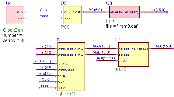
This figure shows our simple controller, which uses a ROM (the iram module) to implement the control signals for the datapath. The PC0 module (program counter) is a simple counter that starts at 0 on reset, and then increments each clock cycle. These actually implement an FSM, where the counter is the state register and next function, and the ROM implements the output functions.

The iram is a table of 16-bit “instructions”, whose format is shown above. RA, RB and RD are the addresses of the A and B source registers of the D destination register. Note that these are 3-bit values, but since we have only 4 registers, we will use only the two low-order bits. The ALU Op is the opcode you used in the design of your ALU.
Construct the simple processor shown above. The file iram0.dat is a text file that
is read by the simulator to initialize the values in the
10110_000_000_000_00 // R0 = 0
10010_001_000_000_00 // R1 = R0 + 1
10011_010_001_000_00 // R2 = R1
10000_001_001_010_00 // R1 = R1 + R2
10011_010_001_000_00 // R2 = R1
10000_001_001_010_00 // R1 = R1 + R2
10011_010_001_000_00 // R2 = R1
10000_001_001_010_00 // R1 = R1 + R2
10011_010_001_000_00 // R2 = R1
Write your own program in a new file that computes the Fibonacci numbers: 1,1,2,3,5,8,13,… The file name is a parameter of the iram module – right-click the module to change the parameter and then recompile.
Turn In
1) Schematic of the register file
2) Schematic of the register file test
3) Console log of the register file test
4) Schematic of your simple processor
5) Printout of your Fibonacci program
6) Timing diagram of the program running, showing the values of the registers
in the register file