CSE370 Laboratory Assignment 1


Constructing Simple Logic Circuits


Distributed: 6 October 2003
Due: 10 October 2003


Objectives

This first laboratory assignment will get you familiar with the prototyping board you will be using the entire quarter.  Your goal will be to realize the Boolean expression you derived for the “jack of diamonds” using simple Boolean logic gates included in your laboratory kit.  By the end of this lab you should know how to construct and verify the operation of a small circuit (3-6 logic gates) using switches and LEDs as I/O devices.


Laboratory Design Kits

The design kits contain everything that you need to construct and test medium size circuits.  We will collect a $100 security deposit check from each student which is returned uncashed at the end of the quarter when the kit is returned.  You will be expected to return the kit in good condition and with everything intact, including the chips.  Included in the DesignKit are:

Digilent XLA5 prototyping board (including a prototype area consisting of a solderless breadboard)
• Power supply
• Logic probe
• Bag of pre-cut pre-stripped wires
• Wire stripper/cutter
Some standard TTL logic chips (all DIP - dual-in-line pin packages - compatible with the breadboard)
• Chip extractor tool (the only way you will remove chips from the breadboard - for the safety of your fingers and the chip's pins)
Please make sure that all of the above are in your kit.  We may provide additional materials later in the quarter.  Most likely, you will also receive some programmable logic devices, a serial cable to connect your board to a PC, and a 2-line by 16-character LCD screen with an 11 pin interface.  You will want to buy a pair of long nose small pliers.  The pliers are invaluable for straightening hook-up wire and bent pins on the chips.  They are also useful for inserting and removing wires in crowded protoboards.

Accidents do happen, so we will replace a certain number of chips whose pins may get bent.  Generally, the first time, most any damage will be forgiven.  However, incidents of gross negligence will not be met with such forgiveness.  In particular, you should pay careful attention to where your power wires are and never allow a short between ground and power supply (GND, 0 volts, and VDD, 5 volts).


XLA5 Prototyping Board

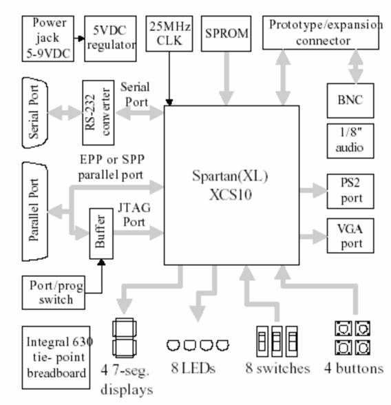
The diagram below shows a block diagram for the entire XLA board.  Note that this diagram highlights the large programmable logic that is on the board.  Your kit does not have this chip in place.  Although, we will use it later in the quarter to provide an environment for the circuits you will design.  You will not be programming this chip in this class, that will happen in CSE467.  For now, your focus will be on the upper right hand corner - the prototyping area.  You will also make use of buttons, switches, LEDs, and 7-segment displays as I/O devices.  For the final laboratory assignment, we will also use the serial port connector, but we'll handle the details of how that get to the prototyping are where your circuit will be.

XLA5 Schematic Block Diagram


Breadboarding Techniques

The breadboard on the XLA board is the large white plastic area in the center of the board and is comprised of 63 rows (numbered 1-63) and 10 columns (lettered a-j) of holes.  On every row, holes in columns a, b, c, d, and e are connected together underneath the white plastic.  So are the holes in columns f, g, h, i, and j.  There are no connections across rows so that all the holes in row 1 are in no way connected to any of the holes in row 2 and so on.  Therefore you can think of the prototyping area as providing 126 (63 rows split in half by the trough) 5-way connectors for wires.  You'll make connections between these 126 regions using the pre-stripped wires in the bag in your kit.  These should be inserted as perpendicular as possible to the breadboard and should slide in and out with just a little force.  If you find that there is a lot of resistance in either direction, then please call over the TA or one of the lab staff.  Do not try to force anything larger than the pre-cut/stripped wires that we've provided into the holes as this could damage the breadboard causing costly repair.  Later in the quarter, you may need more wire.  It will be provided for you at that time.

Before doing any work on the protoboard such as wiring and inserting/removing chips, be sure the power is OFF.  That is, unplug the power connector while you are constructing the circuit.  After you have finished wiring up your design and before you turn on the power, double check the power and ground connections.

Wiring Guidelines

• Arrange the IC chips on the protoboard so that only short wire connections are needed.  Put tightly connected chips closer together.
• Try to avoid a jungle of wires.  Long looping wires that go way into the air are easy to pull out (a hard bug to find later when the circuit doesn't work as intended).
• Try to maintain a low wiring profile so that you can reach the pins of the chips and so the chips can be replaced if necessary.  The best connections are those that lie flat on the board.

Using the Logic Probe

The logic probe provides a very convenient way to check the value of any signal in your circuit.  The probe has two lights, HI and LO, which indicate the value of the signal.  The logic probe responds to the input voltage in two ways depending on whether CMOS or TTL is selected.  We will use the TTL setting which lights the LO light for voltages <0.8v. and lights the HI light for voltages >2.3v.  If neither light is lit, then the signal is floating (ie. not being driven by any active output) or has some value between 0.8 and 2.3v.

The logic probe is also used to “catch pulses”.  If the PULSE MEMORY switch is placed in the MEM position, the PULSE indicator will turn on as soon as a transition, high or low, occurs on the input.  This convenient for determining if a signal changes when the change happens too fast to be visible.  This is useful for detecting glitches.


Tasks

  1. Use your logic probe to determine in which position the switches provide a 0 or 1. 
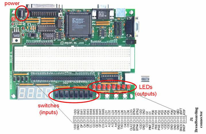
    Remove the power line from the board.  Connect a wire from a switch to the breadboard area - you should probably just use the first switch (SW1).  You can see where to insert your wire into the breadboard connector in the figure below. 

    XLA5 photo

    The large black bar just below the white breadboard area has connections to many of the devices on the XLA board.  The names of the connections points are printed on the board and reproduced below.  Connect another wire into the same 5-hole block and leave its other end dangling so that you can use the probe to touch it.  Connect a wire from VDD to a different 5-hole block that you will use for your 5v source and connect another wire from GND to yet another 5-hole block that you will use for your 0v source.  You may want to choose 5-hole block near the edges of your board.  Place another wire in each of the 5v and 0v regions and leave their other end dangling - but make sure they are far apart and don't ever touch as this will short the power supply and could cause some smoke or bad odor as parts start to burn (should this happen, pull out the power cord immediately).  Clip the probe's two leads to VDD and GND by connecting the red one to VDD and the black one to GND.  This is an important color convention to follow.  You can now connect power to the board.

    Now, touch the probe tip to the dangling end of the wire connected to the 5-hole block where you connected the switch. You should see either the red or green light go on.  Change the position of the switch and note that the light should change as well.  Note which switch position corresponds to hi.
  2. Connect a switch to an LED.
    Pull out the board's power connection before changing anything - safety first (We won't repeat this, but you should always remove power before making any wiring changes and only reconnect it after you've double-checked that you've wired things correctly). 
    You can connect the switch and LED directly by just placing a wire between SW1 and LD1 on the J1 connector.  Alternatively, you could use wires to create connection points in the breadboard area.  Reconnect power and verify that the LED follows the switch.
  3. Place an inverter (NOT gate) between the switch and LED.
    Now, we'll place our first logic circuit onto the board.  Insert a '04 inverter package into an empty region straddling the trough on the breadboard.  Each pin of the chip is now connected to a 5-hole connection block on the breadboard.  Connect wires from the GND and VDD pins of the '04 to the power and ground connection blocks you set up for part 1.  Make sure to get the right pins GND is pin 7, VDD is pin 14 on the '04.  Use the chip maps to ensure you are doing the right thing and to choose a particular inverter of the 6 in this package.  Connect the input of the inverter to SW1 and its output to LD1.  Now the LED should light up when the switch is in the opposite position of part 3.  Connect the output of your inverter into a second inverter's input and connect LD1 to this second inverter's output.  We are now back to where we were before.  Two inverters logically cancel.
  4. Connect a two-input NOR gate to two switches and one LED. 
    Move the switches to all four possible position combinations and verify that the NOR gates works as you expected.
  5. Realize a circuit to detect the "jack of diamonds" using the encoding provided in the solution for assignment #1 part 1.4a (scheme 1)
    You will need to choose the appropriate gates to implement this logic and you will have to do it in pieces as no one gate can implement the function directly.  A suggestion is to implement the "jack" part as one circuit, then the "diamonds" part as another circuit, and, finally, AND the result.  You will use 6 switches and 1 LED for this part.  Use SW1 and SW2 for the suit and SW3 through SW6 for the value.  Show this last circuit to a TA and have them check you off as having completed this laboratory assignment. They may ask you to show them your work and explain your circuit.


Comments to: cse370-webmaster@cs.washington.edu (Last Update: )