CSE370 (Autumn 03) Assignment 5 Solution
1. CLD-II, Chapter 4, Problem 4.20
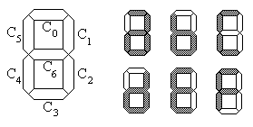
4.20. Extend the BCD-to-seven-segment LCD
to become a Hexadecimal LED display decoder. The LEDs
for 0-9 are the same, and the following diagram shows which segments to
illuminate to denote the hex digits A(1010), B(1011),
C(1100), D(1101), E (1110) and F(1111).
a.
Obtain the minimized sum of products implementations
for the display inputs.
|
A |
B |
C |
D |
C0 |
C1 |
C2 |
C3 |
C4 |
C5 |
C6 |
|
0 |
0 |
0 |
0 |
1 |
1 |
1 |
1 |
1 |
1 |
0 |
|
0 |
0 |
0 |
1 |
0 |
1 |
1 |
0 |
0 |
0 |
0 |
|
0 |
0 |
1 |
0 |
1 |
1 |
0 |
1 |
1 |
0 |
1 |
|
0 |
0 |
1 |
1 |
1 |
1 |
1 |
1 |
0 |
0 |
1 |
|
0 |
1 |
0 |
0 |
0 |
1 |
1 |
0 |
0 |
1 |
1 |
|
0 |
1 |
0 |
1 |
1 |
0 |
1 |
1 |
0 |
1 |
1 |
|
0 |
1 |
1 |
0 |
1 |
0 |
1 |
1 |
1 |
1 |
1 |
|
0 |
1 |
1 |
1 |
1 |
1 |
1 |
0 |
0 |
0 |
0 |
|
1 |
0 |
0 |
0 |
1 |
1 |
1 |
1 |
1 |
1 |
1 |
|
1 |
0 |
0 |
1 |
1 |
1 |
1 |
0 |
0 |
1 |
1 |
|
1 |
0 |
1 |
0 |
1 |
1 |
1 |
1 |
1 |
0 |
1 |
|
1 |
0 |
1 |
1 |
0 |
0 |
1 |
1 |
1 |
1 |
1 |
|
1 |
1 |
0 |
0 |
1 |
0 |
0 |
1 |
1 |
1 |
0 |
|
1 |
1 |
0 |
1 |
0 |
1 |
1 |
1 |
1 |
0 |
1 |
|
1 |
1 |
1 |
0 |
1 |
0 |
0 |
1 |
1 |
1 |
1 |
|
1 |
1 |
1 |
1 |
1 |
0 |
0 |
0 |
1 |
1 |
1 |
|
|
|
|
|
|
|
|
|
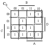
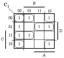
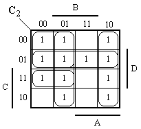
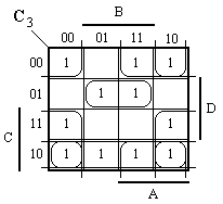
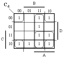
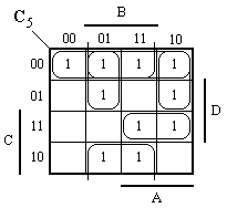
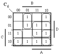
C0 = AD’ + AB’C’ + BC + A’CD + B’D’ + A’BD C1 = A’B’ + AC’D + A’CD
+ A’C’D’ + B’D’ C2 = A’B + AB’
+ C’D + A’C’ + A’CD C3 = AD’ + B’D’ + B’C + BC’D + CD’ C4 = AC + AB + B’D’
+ CD’ C5 = ACD + AB’C’
+ A’BC’ + BD’ + C’D’ C6 = AD + AB’
+ A’BC’ + B’C + CD’ |
|
|
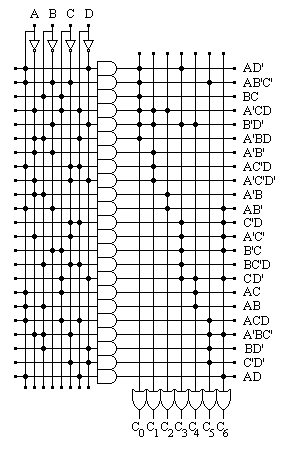
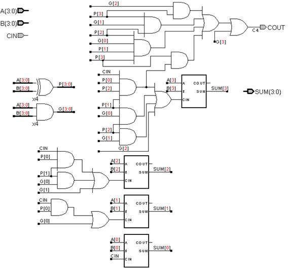
b. Show how to implement the logic
for the extended design as a PLA with four inputs and seven outputs. Draw the
AND array and OR array, and indicate what connections must be made to implement
the function. For each output from the AND array, indicate along the wire the
product term it is implementing.
|
This
implements the converter using the least possible AND gates. In several cases I chose a less than
minimal grouping in the K-map for a given equation to reuse a min-term
between the different functions. If the functions weren’t optimized to
maximize overlap then there would be more AND gates, though some would have
less inputs. |
|
2. CLD-II, Chapter 4, problem 4.28
4.28 Design a combinational logic subsystem with three inputs, I3, I2, I1, and two outputs, O1, O0, that behaves as follows. The outputs indicate the highest index of the inputs that is driven high. For example, if I3 is 0, I2 is 1, I1 is 1 the O1, O0 would be 01 (i.e., I2 is the highest input set to 1).
a. Specify the function by filling out a
complete truth table.
|
I3 |
I2 |
I1 |
O1 |
O0 |
|
0 |
0 |
0 |
0 |
0 |
|
0 |
0 |
1 |
0 |
1 |
|
0 |
1 |
0 |
1 |
0 |
|
0 |
1 |
1 |
1 |
0 |
|
1 |
0 |
0 |
1 |
1 |
|
1 |
0 |
1 |
1 |
1 |
|
1 |
1 |
0 |
1 |
1 |
|
1 |
1 |
1 |
1 |
1 |
b. Develop the minimized gate-level
implementation using the K-map method.
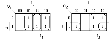
O1
= I2 + I3 O0 =
I2’I1+I3
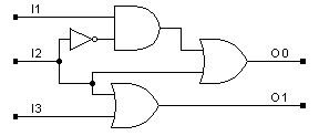
c. Develop an implementation using two
4:1 multiplexers.
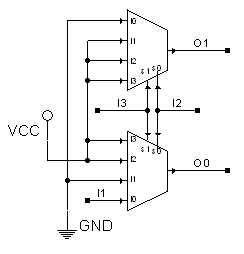
d. Compare your implementation for (b)
and (c). Which is better and under what criterion?
(b) is
better because it uses only 3 gates and 1 inverter. The traditional
gate-level implementation for a 2:1 multiplexer
requires 3 gates and 1 inverter, and (c) would require 6 of these 2:1
multiplexers.
3. CLD-II, Chapter 5, problem 5.2
Design a fully combinational adder/subtractor that can be cascaded to form a multi-bit circuit. The inputs are data inputs A, B, Carry-In CI, and Borrow-In BI. The outputs are data output F, Carry-Out CO, and Borrow from Left BL. A mode input M = 0 indicates addition and M = 1 indicates subtraction. Can the carry and borrow inputs and outputs be combined?
Truth Table:
|
M = 0 |
M = 1 |
||||||||||||||||||||||||||||||||||||||||||||||||||||||||||||||||||||||||||||||||||||||||||
|
|
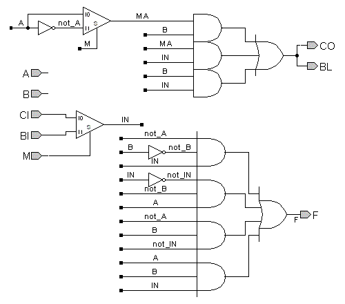
The BL and CO outputs could be combined, as
could the CI and BI inputs. This is possible because only one of each set is
ever in use, determined by the value of M.
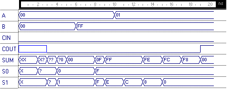
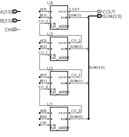
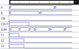
4. Ripple-Carry Adder
Construct a 4-bit ripple-carry adder with four full-adder blocks using Aldec ActiveHDL. First construct - out of basic gates from the lib370 library - a single-bit full-adder block to reuse. Verify your design using simulation, turn in the schematic and timing waveforms showing what happens when you have "1111" and "0000" as the numbers to be added and you change the "0000" to "0001". How long does it take the sum to get to the right value? Repeat this experiment starting with "1010" and "0000" and changing the "0000" to "0101". Explain the differences between the two cases.
Schematic:
Case 1: A=0000, B=1111 changes to A=0001,
B=1111
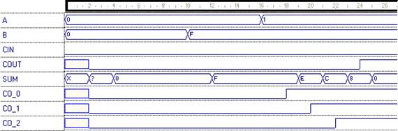
Note the Sequential Rise of the Carry
signals CO_0, CO_1,CO_2
Case 2: A=0000, B=1010 changes to A=0101,
B=1010
The sum takes 9ns for Case 1 and 2ns for Case 2 because Case 1 has to
wait for the carry signal to propagate through all 4 bits. In Case 2, the initial value is correct
because there are no carry outs for any of the bits.
5. Repeat the previous problem but now construct a 4-bit carry-lookahead instead. Use
the same full-adder module as the previous problem. Repeat the two simulations. How much faster is the carry-lookahead adder in both cases? Explain the differences with the result of the previous problem. How do your circuits from this problem and the previous one compare in the total number of gates they use (remember to consider gates in all sub-blocks)?
Schematic:
Case 1: A=0000, B=1111 changes to A=0001,
B=1111
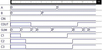
Takes 6 ns (15-9) compared to 9 for the ripple-carry
Case 2: A=0000, B=1010 changes to A=0101,
B=1010
Analysis:
|
|
Cases |
AND |
OR |
XOR |
TOTAL |
|||||
|
1 |
2 |
4 |
3 |
2 |
4 |
3 |
2 |
|||
|
Ripple-Carry |
9 |
2 |
0 |
16 |
12 |
4 |
4 |
0 |
0 |
36 |
|
Carry Look Ahead |
6 |
2 |
2 |
19 |
23 |
6 |
5 |
2 |
4 |
61 |
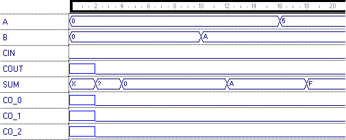
6. Design a 8-bit carry-select adder for unsigned numbers. It should be designed hierarchically at the schematic diagram level and include 3 instances of the 4-bit ripple-carry adder module you created in the previous problem. You'll also need to include some multiplexers. Make sure that your 8-bit carry-select adder also has a carry-out in case anyone would ever want to use it to build a larger adder. Verify its operation for "11111111" + "00000001". Turn in the schematic and simulation waveform
Schematic:
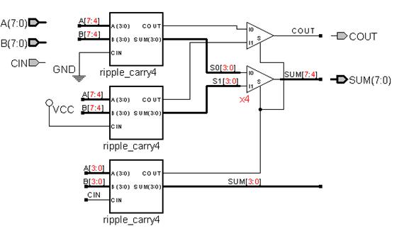
Note: This schematic makes use of buses which are bundles of wires
represented by a single wire. Also, the multiplexer for the sum is a 2:1
multiplexer that has been arrayed to be a 4-bit
2:1 multiplexer.
Waveform: A=00000000, B=11111111 to
A=00000001, B=11111111