This assignment consists of a one larger project. The objective is to expose you to the process of building a complete system from smaller pieces. As in software engineering, you'll have some modules already available and will have to learn how to use them. There will be four modules for which the interfaces are defined to varying degrees and you will have to fill in their internal functionality. We have also provided a test bench for you to use in simulating your system.
To begin, download the project files. Unzip the file on your C: drive so that in the end you have a folder C:\assignment9. This will guarantee that all the Verilog modules in the project will maintain their links to their Verilog source (it has to be in a folder with this name because of DesignWorks' insistence on absolute rather than relative path names).
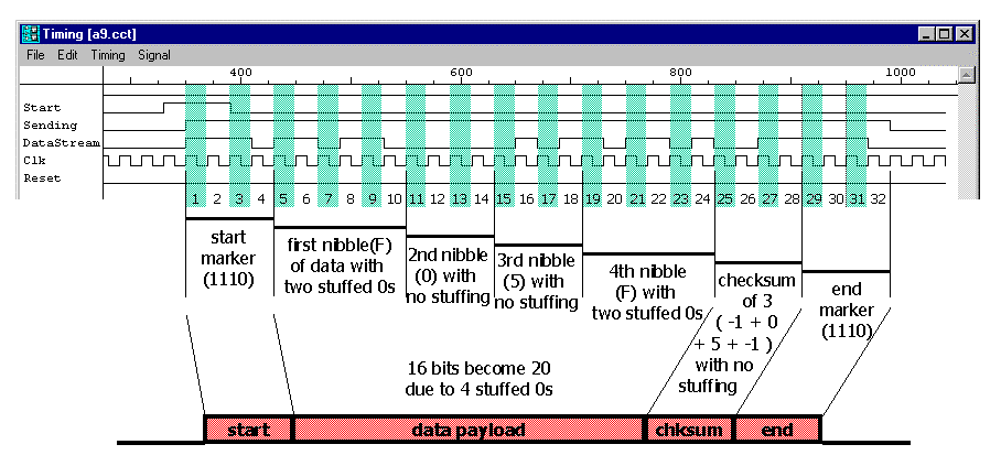
Make sure to take some time to look at all the modules provided. Start up DesignWorks and open the design C:\assignment9\a9.cct which is the high-level block diagram of the project and its test bench. The component at the top of the drawing sheet (labelled Packet Generator) is the test bench. You can set precisely which data bits form the data payload of the packet and whether you would like the packet generated with a bad length or bad checksum (so that you can check your packet receiver). To begin open up the "simulator" tool and the "timing" tool. You should see 5 signals in the timing window (these are the inputs and outputs of the packet generator block). Set the simulator speed to "March" and set the reset switch high for at least one clock cycle (you'll see "Sending" and "DataStream" go from unknown values to zeros). Set the data of the packet to be hex F05F from right to left (note that the most significant bit is on the right). Now, hold down the "Start" push button for at least one clock cycle and you'll see data start streaming out of the packet generator as in the figure below. You'll note that there are not 20 bits between the start and end markers (16 data payload and 4 checksum bits) but rather 24. This makes a total of 32 (24 data/checksum bits + 8 for the two end markers). This is the case because bits are "stuffed" as in your previous assignment. Every time two consecutives 1s are sent, they are followed by an extra 0. This is so that the pattern of the start and end markers (which is 1110) will never occur in the data.

Your task is to design a receiver for these packets. Its architecture is already specified for you and consists of 4 finite state machines and a small data path (see the bottom portion of the DesignWorks schematic). The data path consists of 4 4-bit registers to hold the payload bits of the received packet. Furthermore, you have an ALU (that can perform add, subtract, and pass through operations) and an accumulator register. Together these two components (ALU and accumulator) can be used to check the checksum. All the elements of the data path are stock parts that are completely specified for you as would be the case in industrial practice (check out their Verilog).
Therefore, your job is to use the datapath provided as is and only fill in the internals of the four finite state machines. These will now be described in turn.
The Framer state machine's function is to determine the start and end of the packet data stream. See the figure below for its interface specification. Note the signal Pval (for "packet valid"). This machine will include a pattern detector and a shift register. You must construct this machine using DesignWorks schematics and NOT in Verilog.
The Destuffer state machine's function is to determine that the length of the packet is correct (20 bits = 16 payload + 4 checksum) and signal which 0s are stuffing and to be ignored downstream. See the figure below for its partial interface specification. Note the signal Sval (for "serial valid"). This machine will include a counter and an FSM similar to that of the last assignment. You must design this machine using Verilog.

The S2P state machine's function is to transform the serial data to parallel format and load it into the registers of the data path. Note that this machine could include several shift registers. This would must also be constructed using schematics and NOT using Verilog.
The Chksum state machine's function is to take each nibble through the ALU and accumulator to determine whether the check sum is correct. You will need to use several of the ALU's functions. This machine also signals that it received a packet. At that time, the values of ChkOK and LenOK should be valid. Use Verilog for this machine.
Make sure that your machines are designed so that they only need to be reset once at the beginning and not after every packet.
You should consider each of the four state machines as a separate unit. What we would like to see is a detailed description of the internals of each. For the two that use Verilog, make sure to comment the code and if there is a state machine make sure to include a state diagram (nodes and arcs) whose state names match those in the Verilog code. For the two for which you will use a schematic, include some text that describes why you constructed the circuit the way you did. Finally, you should include a waveform (not $display output) for each machine when your circuit receives a good packet, a too-short packet, and a bad-checksum packet (a total of 12 waveforms - you should be able to fit each one or more than one on a single sheet if you use something like MSWord for your write-up).
Extra Credit:Replace the packet generator with a circuit of your design. Ideally, it would have exactly the same inputs as the block currently there and be decomposed into a set of blocks similar to those of the packet receiver. (This will add 50% bonus points to the grade of this assignment.)
Have fun!