Lab 2: Digitally You
Overview
Now that you have gained some familiarity with Quartus, ModelSim, and the DE1-SoC board, let's develop a SystemVerilog design! This lab will walk you through the design and implementation process.
Instructions
Task 1 – Digit Recognizer (Design)
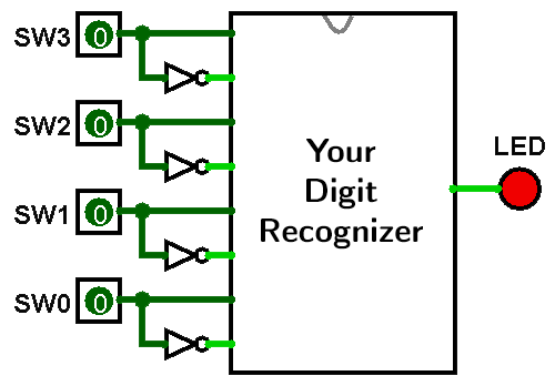
Electronics can be cold and impersonal so let's change that by having your DE1 recognize you! We want to design a circuit that will light up an LED only when you input the last digit of your student ID number. Your goal is to design the circuit out of NOT, NAND, and NOR gates using the fewest number of gates possible. Gates can have at most two inputs.
- Find the last digit of your student ID number in the "Digit" column of Table 1 below – this is known as .
- Design the circuit by hand that will output a 1 only when the switch code matches your particular Digit. Be sure that it also outputs a 0 for invalid inputs (e.g., all switches are 1).
| SW3 | SW2 | SW1 | SW0 | Digit | |
|---|---|---|---|---|---|
| 0 | 0 | 0 | 0 | 0 | |
| 0 | 0 | 0 | 1 | 1 | |
| 0 | 0 | 1 | 0 | 2 | |
| 0 | 0 | 1 | 1 | 3 | |
| 0 | 1 | 0 | 0 | 4 | |
| 0 | 1 | 0 | 1 | 5 | |
| 0 | 1 | 1 | 0 | 6 | |
| 0 | 1 | 1 | 1 | 7 | |
| 1 | 0 | 0 | 0 | 8 | |
| 1 | 0 | 0 | 1 | 9 |
inside the Digit Recognizer count towards your total "gates used."
Only use the input NOT gates that help you simplify your design.
Task 2 – Multi-Digit Recognizer (Implementation)
Recognizing only one digit is a bit simplistic, so we’d like to scale it up to handle more digits.
- Copy your Lab 1 project folder (or unzip a fresh copy of ) into a new Lab 2 project folder.
- Download lab2.sv
(code) into your Lab 2 project folder, add
it to your Quartus project, and set lab2.sv as your
top-level module.
Note that we are giving you a pre-written test bench!
Note that the testbench uses an "initial" statement to generate the input patterns, with #10 delays and a for-statement. However, the testbench is non-synthesizable (i.e., the code doesn't have a physical hardware interpretation and is therefore only useful/meaningful in simulation).
- Draw a block diagram for a module that
recognizes the last two digits of your student ID
number. It has takes 8 inputs, SW7-SW0, and has one output, LED0.
SW3-SW0 will be the rightmost digit, encoded as
in Task 1, and SW7-SW4 will be the next digit,
using a similar code (e.g., the digit 8 is encoded as
SW7=1, SW6=0, SW5=0, SW4=0).
Draw the diagram before you write any code. This block diagram should be a box that is labelled with your Verilog module's name with wires entering/exiting it that represent the module's ports. These should be exactly as you see them in the code. Label multi-bit signals (busses) by putting a slash/through them and writing their bit width. You're free to choose whether to represent an N-bit input with a single slashed line, or N separate lines.

Inside of this box, draw the wires and gates that you will use to implement your functionality. If you are going to use any non-boolean-logic operators like+or==, represent them as a block in the diagram with their inputs and outputs clearly labelled:

If you are going to use any muxes, draw them as trapezoids described in lab 1.
If there is anything else you're not sure how to draw, just make a choice about how to show it and then explicitly label what it means (when in doubt, write it out). - In lab2.sv, translate your block diagram into SystemVerilog code. Make sure to test your design in simulation BEFORE loading it onto the FPGA.
Grading
Deliverables
Submit a zip file containing your lab report and finished/modified source files on due on Wednesday April 16 at 2:30 pm.
Your zip file should contain:
- lab2_report.pdf
- a modified/updated lab2.sv
Working Design
44 points for correctness, style, and testing.
Logic Minimization
Up to 10 points for using as few logic gates as possible in Task 1.
Each gate (NOT, NAND, NOR) counts the same, though any NOT gates connected directly to a switch input are not counted. Gates can have at most two inputs. The fewer gates, regardless of the number of chips, the better the grade.