Lab 1: An Introduction to SystemVerilog & Digital Components
Overview
The first lab will introduce you to the Altera’s Terasic DE1-SoC development board and our primary design tool this quarter, Intel's Quartus Prime. These components are very important for all future labs so please pay attention. This lab outlines our expectations for reports and demos.
Instructions
Task 1 – SystemVerilog Design and Simulation
The designs in this class will be done through the Intel Quartus Prime software. This is preloaded on machines in the lab (CSE 003), and you are free to do all the work on these PCs. However, you can install the software on your own computer, if desired, by following the page.
Open the and complete Sections 0 through 8. Please ignore references to the *_tb.sv files in sections 2.2, 7.1, and 7A.1. Be sure to do all of the steps and ask the course staff for help when you encounter issues.
- Save a good screenshot of the simulation waveform from your mux4_1 testbench. Make sure all the signal waves and names are visible (or scroll the waveform and take multiple screenshots if necessary). Include this in your lab report. During your lab demo, you will need to show these screenshots to a TA and explain what they mean.
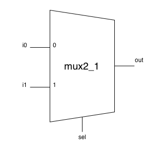
Now let's draw some block diagrams. The following mux2_1 diagram shows its two data inputs, select input, and output. The 0 and 1 written inside the trapezoid show which input is chosen for each value of the select signal. Look at the mux2_1 module and compare it to its schematic symbol.
- Draw a schematic for a mux4_1 built from three mux2_1 instances. Use the exact signal names from the given module when labeling your schematic. (i.e. The inputs should be labeled i00, i01, etc.). Put this drawing in your lab report.
Task 2 – Logic Investigation
Read through the document. Make sure you know where the LEDs, switches, and push buttons are on the DE1 and then connect it to your computer and power on your board. Feel free to play around with preloaded program to get a feel for the board inputs and outputs.
Now finish the rest of the Quartus Tutorial to program your board with the provided top-level module lab1.sv (code). Refer to the code comments and play with the appropriate inputs to discern the logical behaviors of our input and output signals.
Answer:
- Which logical value (0 = FALSE = GND, 1 = TRUE = VDD) turns the red LEDs on?
- Which position (up or down) of the slider switch outputs a TRUE?
- Which position of the push button (pressed or unpressed) outputs a TRUE?
Task 3 – Add Simple Logic
Now modify lab1.sv to implement the following additional logic. You will only need to add one line of code beneath each TODO comment. Refer to Lecture 2 for the syntax for gate modules and logical operators.
- Place an inverter (NOT gate) between SW2 and LEDR4.
- Use a second inverter to connect the output of the first inverter to LEDR5.
- Place a two-input NOR gate between two unused switches and an unused LED (your choice).
Re-synthesize your modified project and load it onto your board to make sure that it behaves as you would expect. Don't forget to upload your modified lab1.sv alongside your lab report.
Lab Deliverables & Grading
You can earn up to 48 points for correctness, style, and testing.
Gradescope Submission
Submit a zip file containing your lab report and finished/modified source files on due on Wednesday, April 8 at 2:30 pm.
Your zip file should contain:
- lab1_report.pdf, with the contents described below
- lab1.sv (5 pts)
Lab Report
Your report should contain the following:
- From Task 1:
- A screenshot of the ModelSim simulation for the mux4_1 circuit. (4 pts)
- A simple, accurate explanation of what the mux4_1
circuit does. (2 pts)
Note: We do NOT want a written description of the circuit gates, we want a description of what it actually does – if you're not sure, see how we described how the mux2_1 circuit works in Section 2 of the Quartus Tutorial.
- Your drawing of the mux4_1 circuit. (2 pts)
- From Task 2:
- The value of the signal (TRUE or FALSE) that makes the LEDs light up. (4 pts)
- The position of the switches (up or down) that cause them to output TRUE. (4 pts)
- The position of the push buttons (pressed or unpressed) that cause them to output TRUE. (4 pts)
- From Task 3:
- N/A (Task 3 has no report component)
- How many hours (estimated) it took to complete this lab in total, including reading, planning, designing, coding, debugging, and testing. (1 pts)
Lab Demo
Demos are due during your assigned slot. Rescheduling is only permitted if you turned your lab report in later than your demo time or have extenuating circumstances and prior approval by course staff. In any case, it must be completed by end of day Friday of the week your lab report was submitted.
- Demonstrate and explain your working simulation of the mux4_1 circuit. (4 pts)
- Show and explain your diagram of the mux4_1 circuit. (4 pts)
- Demonstrate your working NOR (4 pts) and double inverter circuits. (4 pts)
- Answering conceptual questions about your design and implementation. (4 pts)
- Professionalism and conduct (5 pts)
How to Demo
Preparing & Setting Up:
- Show up early to set up.
- Synthesize your bit files ahead of time. This can take 5+ minutes for later projects, so don't waste demo time doing it.
- Verify your simulations look correct and your project loads onto the board properly.
- Bring a pencil and paper for conceptual questions.
- Only add yourself to the queue once you are fully ready; include your demo time slot in the description.
During Your Demo:
- Once your demo starts, you may not edit files or fix bugs. You are graded on what you have completed at the start of the demo.
- Do your best to answer conceptual questions and walk through your thought process. Conceptual questions are graded on effort and understanding, not completeness.
- Be prepared to explain your waveforms without referencing your report or code.