Lab # 3
DUE: In one week, at 1:30 pm
Collaboration Policy:
Unless otherwise noted, your group may collaborate with
other CSE467 groups on the lab assignments. Collaboration means that you
may discuss the experiments and make notes during the discussion, but you
may not copy another groups work when doing the experiments; you may not
copy experimental results from another group; and you may not copy any
part of another groups lab report. In addition, every individual in a
group must understand the experiments, must participate in the writeup,
and should understand the results. Collaboration does not mean that one
person may perform the experiments and another write up the resultsall
lab partners must share equally in all parts of the lab assignment.
Late Policy:
The lab assignments are due in one week, at the beginning
of your lab section. Assignments handed in after lab will incur a 10% penalty;
the penalty will increase by 10% for each additional day late.
Overview:
The purpose of this lab is to give
you experience using the Xilinx Foundation tools. When you have completed
this lab, you will know how to:
Create a new project in Foundation.
Draw schematics for your circuit using
hierarchy.
Simulate your circuit using the Foundation
simulator.
Download your circuit to a Xilinx
chip on the XESS
board
View and print schematics and simulation
results.
The lab:
Answer all the questions in this handout in your lab
writeup. Show all of your work, and remember, your solutions must
be legible. The points for each problem are noted on the problem statement.
The Xilinx Tutorial:
The CAD tool that we'll be using this quarter is from
Xilinx and is called Foundation. The top-level tool from which you call
all the other tools is Foundation Project Manager. From there you can fire
up the schematic editor, simulator, state machine editor, and the tool
that maps the design to the Xilinx FPGA. The Foundation software is loaded
in the hardware lab (Sieg 327), and in the PC labs (Sieg 232 and 329).
Note: Although you can do the software part of this lab in 329, the machines
in 327 are the only ones that have the parallel-port drivers needed to
support the XESS board. Do not remove the parallel cables or the XESS boards
from the lab.
In lab2, you worked through the first two parts of a tutorial
located here.
In this lab you will use the Foundation tools to create a design and map
it to the Xilinx chip on the XESS board.
Simulation Scripts:
There is one very useful feature of the simulation tools that isn't covered well in the tutorial, and that is the use of simulation scripts. Although you won't be using scripts in this lab (we will use them in lab4), we mention them now so you can at least think about them when using the tools. When using a simulation script, you write a set of test cases, and then the simulation tools can automatically check that your design is correct (at least in terms of your simulation script), saving you a lot of work. This can be much easier than the "traditional" method of providing stimuli and checking waveforms by hand each time you change your design! For this reason, we'd like you to use simulation scripts for the majority of your testing this quarter (or at least for what you turn in).
The easiest way to learn how to write script files is to look at some examples. A couple of example you should find useful are this template script and this commented example script. Skim through both scripts, and read the comments. The template script contains sections for most of the important script commands you'll be using, while the second script contains a lot more commented examples. When you're (eventually) ready to create your own script file, you need to select Tools -> Script Editor from the simulator. To execute a script file, you need to choose File -> Run Script File (again from the simulator). You can also run a script file right from the script editor, using the restart and start buttons.
After you've finished looking over the example scripts,
go into the Script Editor, and select Help -> SIM Macros Help ; then click
on the Help Topics button. This is the reference guide for all the commands
you can use in your script. If you ever need more detailed information
about a command, this is the place to look. Take a moment to look-up some
of the commands that are in the template file, such as the check, assign,
and cycle commands.
In this lab you will design and implement a complete circuit
using the Xilinx chip on the XESS board and some discrete components on
the protoboard. The circuit is a 1-hot counter that increments (counts
up) whenever it detects a rising edge on its input. You will display the
count value using the 7 LEDs on the 7-segment display on the XESS board.
The input will come from a pushbutton switch on the protoboard. Mechanical
switches do not generate clean logic outputs when they toggle, because
the switch contacts actually bounce open and closed a few times before
settling. In the first part of the lab, you will count these bounces using
the edge counter. In the second part of the lab you will debounce the switches
using a couple of gates (you will build an RS latch using discrete gates).
Edge Counter:
Use the Xilinx Foundation tools to design a 7-bit, one-hot edge counter. Your circuit should have two inputs: A data input that comes from the switch and contains the edges we are looking for, and a reset input to reset the counter. For this lab, do not use any LogiBLOX components. Instead, design your 1-hot counter from scratch using gates and registers from the Xilinx library.
Simulate your design first to make sure it works. The
following section will describe how to connect your circuit to the appropriate
Xilinx chip pads so that you can implement and test it on the XESS board.
Implementing the circuit:
To actually download your circuit to the Xilinx XESS board, you need to first produce a "bitstream file", and then download this file into the XESS board. Here's how:
After you have designed and simulated your circuit, you
are ready to add the elements necessary for implementing it on the XESS
board. You first need to add the following symbols to your schematic:
1. Any inputs to your circuit must go through
an IPAD symbol and then an IBUF symbol.
2. Any outputs from your circuit must go through
an OBUF symbol and then an OPAD symbol.
3. If you use a system clock, it should use a
BUFG symbol instead of an IBUF symbol.
In addition to PADs and BUFs, you need to tell the Xilinx tools how to map your inputs and outputs to actual pins on the Xilinx chip. The most common way to do this is to use a User Constraint File (UCF). The format of a UCF is fairly simple; you simply specify which net names (from you schematic) should get mapped to which pins on the XESS board. For more details, take a look at this example UCF. You will probably want to use this file in your designs, since some outputs (such as for the LED display) must be mapped to particular pins on the XESS board, and our example file already takes care of these things.
To use this UCF in your project (instead of the default one Xilinx creates), first copy it to your project directory. Then go into the Project Manager, select Implementation -> Implementation Options, and choose this constraint file. You can edit the UCF file by double-clicking on it in the Project Manager. To modify our example UCF for your own use, just uncomment the lines that pertain to your design, and add any additional pin mappings that you require. In addition, you need some way to tell Xilinx which PAD/BUF in your schematic corresponds to which net name in your UCF. To do this, simply name the wire between the desired BUF and PAD (in your schematic), giving it the exact same name (case-sensitive!) as the corresponding net name in the UCF. Note that bus names can be given as either X[2] or X<2> in the UCF file.
The UCF contains lines for the pins connected to the 7-segment display. Use these pins to connect the 7 outputs of your circuit. Then add two lines for the data input and reset inputs for your circuit and assign them to pin 27 and pin 28.
There is an alternative way of specifying pin mappings
that you may wish to use. To do this, your first double-click on an IPAD
or OPAD in the schematic to bring up its Symbol Properties dialog box.
Under Parameters, enter LOC for the name, and Pxx for the
Description (where xx is a pin number, from 0 to approximately 84).
Then click on Add, and close the window. This alternative method can be
convenient for user-definable pin locations, but for signals that need
to be mapped to specific pins on the XESS board, using the UCF is probably
safer.
Downloading the Circuit to the XESS Board:
After you've added the necessary pins and labels, you are ready to run the implementation phase of the Xilinx tools to produce a bitstream for the Xilinx FPGA. Go to the Project Manager and click on the Implementation button. In the dialog box that appears, select 4010XLPC84 for the device, and '3' for the speed. If you don't see this device, then go back to the File menu and change the Project Type to use the 4000XL series parts. Click on the Run button. The Xilinx tools will start going through a five-phase implementation process.
At this point, it is possible you will get warnings or errors that you will need to look at carefully. To view the report file, select the Reports tab from the Project Manager screen, and then double-click on Implementation Report Files. If you get any errors, check the implementation report; you most likely just need to go back and tweak some things related to the I/O BUFs and PADs, or perhaps the pin assignments in the UCF.
The implementation phase, once successful, will create a bitstram (.bit) file in your project directory. (Note: if you need to use an older .bit file, it will be located in a \verXX\revXX subdirectory, because Xilinx automatically creates a new version and/or revision each time you complete an implementation phase. The current version of your project can be found by looking on the Project Manager screen, right above the Design Entry button).
Once you have the bitstream file, you can download it
to the XESS board using the 'xsload' program (located in 'd:\xstools\bin\').
This program downloads a bitstream onto the XESS board through a parallel-port
cable that you plug into the PCs. To use it, simply connect the XESS board
to your PC via the parallel cable, and plug-in the XESS board's power cord.
Then run the xsload program from the Windows command prompt, giving it
the name of your .bit file as an argument. That's all there is to it! The
PCs in the lab are the only ones that have the xsload software installed,
so you should not remove the parallel cables or the XESS boards from the
lab.
Testing Your Circuit:
To test your circuit, you will need to place two push-button
switches on the protoboard, and connect them to the XESS board. PLEASE
READ THE INSTRUCTIONS on using the protoboard, contained in the Design
Kit web page. For this lab, you should pay particular attention to
the section on switches.
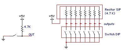
Using the push-button switches:
We will use two push-button switches to provide the two inputs to your counting circuit. Find the pushbutton switches in your Design Kit that have three terminals. One of these terminals is a "common" terminal while the other two are "normally-closed" (NC) and "normally-open" (NO). When the switch is not being pushed, it is in the open state. In this state, the common terminal is connected to the NC terminal. When the switch is being pushed, the common terminal is
connected to the NO terminal. Use the multimeter to determine which terminal is which by measuring the resistance between the terminals.
Using either a resistor pak or a discrete resistor, connect the push-button switch as shown in the figure above, using the "normally-open" terminal so that the connection is made when you push the switch. The output of this switch should then go through an inverter in an 74LS04 chip. See the '04 data sheet to see how the inverters are connected to the pins of this chip. Remember to connect Vdd and GND to the '04 chip, and add a decoupling capacitor across Vdd and Gnd. The output of the inverter should be a logic 1 when you push the button, and a logic 0 otherwise. Test this using your oscilloscope.
Repeat this process with the second push-button switch so that you now have two switches connected up. The next step is to connect these two switches to the inputs of your circuit in the Xilinx chip. This means that you will need to connect the XESS board to the protoboard. When you do this, you will be using one power supply for the protoboard and another power supply for the XESS board. To make this work without ruining things, you MUST CONNECT THE GROUNDS BETWEEN THE TWO BOARDS. Otherwise there will be no common ground reference between the two boards, and the logic levels on one board will be meaningless to the other board.
First disconnect all power supplies from the protoboard and the XESS board. The XESS board should be already be inserted into a protoboard to make it easy to connect to pins of the XESS board, which are connected to the Xilinx chip pins. The pins of the XESS board are numbered from 1 to 84, counter-clockwise around the board, starting in the center of the left-hand side of the board, down to the bottom pin (pin 21) then up the right-hand side of the board from pin 22 to 63, then down the left-hand side of the board from pin 63 to 84.
IMPORTANT: Connect pin 52 (GND) of the XESS board to a GND bus on the Design Kit protoboard. Before you plug power into the XESS board, double-check to make sure that you have the GND signals connected correctly. Use the multimeter to measure the resistance between the grounds on the two boards it should be 0. Also measure the resistance between Vdd and GND on the two boards it should be very high (e.g. high enough not to register).
Next connect the two switches to pins 27 and 28 of the XESS board, which are connected to pins 27 and 28 of the Xilinx chip.
Now plug power into the XESS board and download and try
out your circuit. Each press of the switch should give you a random number
of counts because of the bouncing in the switch.
Debouncing Switches:
You can debounce a switch by using an RS latch and using both the normally-open and normally-closed terminals of the switch as shown in the figure below. The first contact of the switch terminals will cause the latch to change state. Then, even if the switch bounces, the latch will stay in the same state. Use a 74LS00 chip to implement the switch debounce circuit.

Reconnect the data input switch so that it is debounced
and test your circuit to see if the debouncing worked. Remember to disconnect
power before you start rewiring your circuit!
Turn In:
1. Schematics and simulation results for your
edge-counter.
2. How many bounces do you count on average for
your switch?
3. Demonstrate both the un-debounced switch input
and the debounced switch input to the TA and have them sign off on your
schematic.