UW CSE
Winter 2004
CSE467 Advanced Digital Systems Design
Lab # 3
DUE: In one week, at
Collaboration Policy:
Unless otherwise noted, your group may collaborate with other CSE467 groups on
the lab assignments. Collaboration means that you may discuss the experiments
and make notes during the discussion, but you may not copy another
group’s work when doing the experiments; you may not copy experimental
results from another group; and you may not copy any part of another
group’s lab report. In addition, every individual in a group must
understand the experiments, must participate in the writeup, and should
understand the results. Collaboration does not mean that one person may perform
the experiments and another write up the results – all lab partners must
share equally in all parts of the lab assignment.
Late Policy:
The lab assignments are due in one week, at the beginning of your lab section.
Assignments handed in after lab will incur a 10% penalty; the penalty will
increase by 10% for each additional day late.
Overview:
The goal of this lab is to make you familiar with the Xilinx Virtex1000 FPGA
prototyping board. You will start by compiling and loading a simple design we
will give you onto the board. You will then connect a keypad and 7-segment
display to the Virtex1000 FPGA and implement a design in the FPGA that displays
the letter of the key that is pressed.
This lab has four sections. You should be able to complete the first three sections in lab, but the 4th section might take a bit longer.
Part 1 : Setup the Virtex1000 Board
The XCV1000 board will be setup on your lab bench, connected to the power supply and the programming pod. This board has a Virtex1000 FPGA in a socket that allows it to be replaced. You should have no reason to remove the FPGA, but if you do make sure you do not press down on the FPGA when closing the socket.
Power
The power supply provides 5v, 3.3v and 2.5v as well as GND. When you start, the power supply and the board power switch should be turned off. First, turn on the power supply and measure the voltage of each of the power inputs to the board using the multimeter to make sure they are correct. You can then turn on the switch on the XCV1000 board. But turn off the power supply before you do any wiring between the XCV1000 board and the protoboard.
Connecting to the
Protoboard
You will be using the protoboard to implement input and output devices for the FPGA. The pins of the FPGA are 3.3v TTL compatible. This means that you can use 3.3v or 5v HCT logic chips. For this lab, we will not need any chips and we will run the protoboard at 3.3v.
Turn off the power supply Connect power to the protoboard from the power connector on the XCV1000 board using two wires, one for 3.3v and one for GND. It is very important that you connect the GNDs of the two boards together!! It’s always a good idea to use a multimeter to make sure that the GNDs are indeed connected before you turn on the power.
The FPGA pins used to connect to the protoboard will be described in the next section. These pins are made available through the 6 rows of headers. You can use the usual protoboard wires to make the connections. Make sure you turn off the power before doing any wiring.
Part 2: Compiling and Programming for XCV1000bg560
Create a workspace
- Open Active HDL
- Select the option to create a
new work
- Enter your work
- The path to the work
- Do not save on the lab machines hard drive: they will get erased when you log off
- Press OK. Active HDL will
create your new work
- Check the Add existing resource files bullet
- Click Next
- Click Add Files…
- Use Flash_LED.v
- Click Next
- Set the options for the New Design Wizard as shown in
Figure 1 and hit Next
- Enter your design name, click Next and Finish
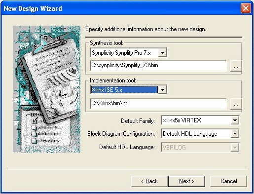
Figure 1
Synthesize
- Select the design flow window
- Select synthesis options
- Select the highest level verilog in the Top-Level Unit box
- Change the Family to Xilinx5x VIRTEX
- Change the Device to V1000bg560, the V1000 part in the Ball grid array package
- Change the Run Mode to GUI
- Press ok, and press the Synthesize button
- Press Run after Synplicity opens up
- After a few seconds, if everything goes right, it will display Done!
- Synpliclty is a very useful tool if you know how to use it
- Click the View Log button on the left-hand side of the screen to view a detailed timing report
- You can see how your design is laid out in two different views
- From the HDL Analyst menu, select RTL > Hierarchical View
- From the HDL Analyst menu, select Technology > Hierarchical View
- After you spend a little time playing with Synplicity, close out of it
- Press the refresh file list button
- Hit the “…” button to the right of Netlist:
- Select the current .edf file and hit Open then Ok
- The question mark next to the Synthesis button should now be a green check
Implement
- Save Generic_Pin_List.ucf in your design folder
- Select options, to the left of implementation.
- Change the Run Mode to Batch
- Select the Translate tab
- Deselect Use default UCF file
- Press the Browse button on the top right
- Select the Generic_Pin_List.ucf file and press Open
- Next, select the Timing and Configure tab
- Change the Simulation Output Format to None
- Check the Generate Bit File bullet
- Press OK
- Press Implementation
- Close the implementation window when it finishes
Program
- Click on the Analysis button and open iMPACT
- Check the parallel cables and make sure your FPGA is plugged in and powered up
- The light on the programmer will be green if everything is okay
- iMPACT will eventually start up, and present you with a wizard
- Select Configure Devices, then Next.
- Select Slave Serial Mode, then Finish.
- An Add Device window will pop up.
- You need to choose the .bit design file, which is located in: <design_name>\implement\ver1\rev1\
- Press Open
- An icon representing your design will appear.
- Right-click the icon and click on Program…
- If everything went right, iMPACT will display Programming Succeeded.
- The Done led on the Xilinx board should be lit and the AJ2 led should be flashing
Editing the Pin Constraints
- Before you can program the FPGA with your keypad-to-led circuit, you need to update the pin constraints file
- You can edit the Generic_Pin_List.ucf file with any text editor
- The file already contains all of the pins that are available for input/output on the XCV1000
- You will need to assign a free pin to all of the input and outputs you have defined in your top-most module
- XCV1000-Pin-Layout has a graphical display of the XCV1000’s pins
Part 3 : Keypad to 7-segment display design
Before you make your design, you will have to understand how the keypad works. The keypad has 16 keys and uses 8 outputs to encode which key has been pressed using two 4-bit unary row and column numbers.
You will find 9 pins on the keypad: 8 of these pins are connected to two sets of 4 wires R[3:0] and C[3:0]. The 9th pin is connected to a special, “common” wire. R[3:0] runs horizontally, one wire per row and C[3:0] runs vertically, one wire per column. The key at row and column (i, j) is at the intersection of wires R[i] and C[j]. (Rows and columns are numbered from 0 starting at the upper-left key.) Pressing the key at location (i, j) causes the wires R[i] and C[j] to be connected to this common wire. Your first task is to use a multimeter to figure out which pins are R[3:0], C[3:0] and common.
1. Draw a figure that labels the keypad pins. Include this figure with the material you hand in.
Before you wire up the circuit, first make sure power has been disconnected. The first thing you do should be to make sure you connect the GND of the protoboard to GND of the Virtex1000 FPGA. See the instructions in the first two parts. To use the keypad, you will connect the “common” pin to GND and each of the 8 R[3:0] and C[3:0] outputs to Vdd through a 4.7K resister (using a resistor pack). This makes the 8 outputs “assert low” outputs: if no key is pressed, all outputs are pulled high. If a key is pressed, two wires are connected to GND, and those outputs are pulled low. Wire up the keypad on the protoboard and connect the 8 outputs to the Virtex1000 FPGA using pins from the pinout file. Wire up a 7-segment display on the protoboard as in Lab 2 and connect the inputs to the Virtex1000 FPGA.
Now design a Verilog module that converts the 8-bit output of the keypad to the appropriate encoding for the 7-segment display. You should break this design into two submodules. One module converts the 8-bit output of the keypad to a 4-bit code plus a “key-pressed” aka “valid” signal. The second module converts the 4-bit code and valid signal into the appropriate 7-segment code. Make sure you code for all 16 keys. Compile this module for the Virtex1000 chip according to the directions in Part 2 and assign the FPGA pins using PACE as you wired them the FPGA to the protoboard circuit.
Have the TA check out your connections before you power on your board.
Now download the bit file and test it out.
2. Demo your circuit and turn in
your Verilog design with the TA’s signature that it works correctly.
Part 4 : Key chords
What happens if you press two keys simultaneously? Assuming that the two keys are on the same row, design a Verilog module that converts the 8-bit code from the keypad into a pair of 4-bit codes and valid signals. If only one key is pressed, then only one output valid signal is asserted (always the some one). Add a second 7-segment display to your setup. Compile, download and test your design.
3. Demo your circuit and turn in
your Verilog design with the TA’s signature that it works correctly.