Problem 1, Digital Camera Design (20pts)
Complete the schematic for this digital camera (this is a
purely qualitative exercise). The black circles indicate missing connections. Your
job is to choose the most appropriate way to interface the device to
microprocessor and to fill any other necessary devices that are missing
including those needed for protection. Missing components might include analog
amplifiers (single-ended or differential), plain wires, resistors, capacitors,
inductors, diodes, and transistors. The shutter is open when the coil is
energized and closed otherwise. Give a sentence or two to explain each choice.
You don’t need to give sizes or values for the components. Assume that the
microprocessor is a variant of the 8051 that has two analog inputs with
internal analog to digital converters. You cannot assume that the analog inputs
are high impedance.
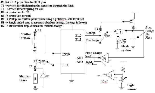
Common mistakes:
Use of OP-AMP as a power device for driving the coil or for
controlling the transistors.
No amplifier, or under-specified amplifier on analog inputs
Lack of protection for coil, 8051 pins.
Attempting to power the coil or flash from 8051 pins or from op-amp.
Direct connection of the shutter button to the shutter drive (no points taken
for this)
Use of FET instead of BJT in discharge circuit. This would technically be
correct if the flash is above rather than below the device. It might even be a
better circuit. (No points taken for this).
Thinking that the motor drive and the coil are somehow separate. The coil is
the drive.
Acceptable alternatives:
Use of FET instead of BJT to drive coil and flash
Use of button as pull-up w/ a pull down resistor instead. This is not as good
because chip can be damaged if programmer writes a zero to the pin!
Direct control of shutter drive from shutter button. This does not make much
sense, but hardware interlocks can be included to prevent picture under low
light conditions.
Problem 2: Microcontroller Memory Architecture
A. Explain what the C compiler would have to do to convert this code into 8051 assembly by showing all the necessary segment declarations and explain what goes into each segment. Yes…it is possible. Don’t worry too much about using proper 8051 assembly instructions and directives; just provide pseudo-assembly code for the contents of any code segments, but make sure you are clear about addressing modes and intent (use comments if necessary). (20 pts)
unsigned byte
table[8] = {1,2,3,4,5,6,7,8};
int i;
void main()
using 0 { // tells compiler to use
register bank 0
while (1)
for
(i = 0; i<8; i++) {
table[i] = table[i]+1;
P1_0 = ~P1_0;
}
}
// defines interrupt function for external interrupt INT1
void
external_handler(void) interrupt 2 using 1 { // register bank 1
P1_0 = ~P1_0;
}
B. Draw the expected waveform on P1.0 if external interrupt
int1 were enabled. Assume that the time
between dotted lines is equal to one iteration of the inner loop, which is
equal to the execution time of the external interrupt handler. (10 pts)
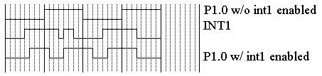
Commong mistakes: not accounting for the delay imposed on the main loop by interrupt processing.
Part A Solution
Common mistakes:
Attempting to initialize the table
in the DATA segement instead of in software in the CODE segment
misuse of addressing modes and memory spaces in expressing Tabel[i]= Table[i]+1
Attempting to write to table[] after declaring it to be CONST or CODE
Failure to initialize the stack
Enabling interrupts….this is not
implied by the C-code (no points taken for this)
use of MOVC instruction for accessing DATA (no points taken for this)
Alternative: this could have been done using only registers and no data segment for the table. You still would
Have to initialize the table in code.
Segments needed
IDATA for STACK
DS 2 Bytes (I think that is more than enough
IDATA for TABLE
DS 8 Bytes
// reset vector
CSEG AT 0
JMP INIT
// external interrupt 1 vector
CSEG AT 000BH
JMP ISR
CODE RSEG for MAIN
Main: MOV R1,#table; // start at table[0]
Loop: INC @R1;
INC R1;
CJNE R1,#table+8, Loop
ORL P1,1;
JMP Main;
CODE RSET for INIT // could be combined with MAIN segment.
INIT CLR PSW; // set register bank to 0
MOV SP, #STACK-1; // initialize stack
MOV R1,
#table // initialize the data
table
MOV @R1,#1;
INC R1;
MOV @R1,#2;
…
MOV @R1,#8;
JMP Main;
CODE for interrupt handler
ISR: ORL P1, 1; // no need to protect or modify PSW. Using compiler directive ignored.
RETI