
Up until now we have been working with basic circuits where the tolerances have been so low as to not cause any analog effects to appear. This lab has two purposes: (1) to give you a sense of the true nature of digital designs (which are never as ``digital'' as they appear; and (2) to give you a working familiarity with the oscilloscope -- a very important piece of test equipment.
For this lab you will NOT be using your usual breadboards. We are intentionally going to drive circuits in this lab to +15V DC. This is 3-5 times higher than you have been using. For this reason the lab staff will provide you a blank bread board with no other components on it.
|
|
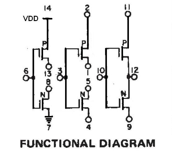
For this lab we are going to be using the CD4007 chip. This chip provides 3 "raw" NMOS and 3 PMOS transistors (Simplified Diagram Below). Your first task is to use 4 of the transistors on this chip to wire up 2 inverters. Recall that an inverter requires a single NMOS and a single PMOS transistor to build. Build two of these and wire the output of one to the input of the other. Connect the output of the second inverter to a 30K (or so) resistor. Ground the other end of the resistor. This last part is important. Without a pull down the output will ``float'' and the measurements you make later in the lab will be impossible
The power supply has two sets of knobs, and we'll be using only the left set. MAKE SURE THE POWER SUPPLY IS DISCONNECTED FROM THE BREADBOARD, and turn on the power supply.
Turn the current knob until the green LED next to the voltage knob lights up. Now set the voltage to 5V using the voltage knob.
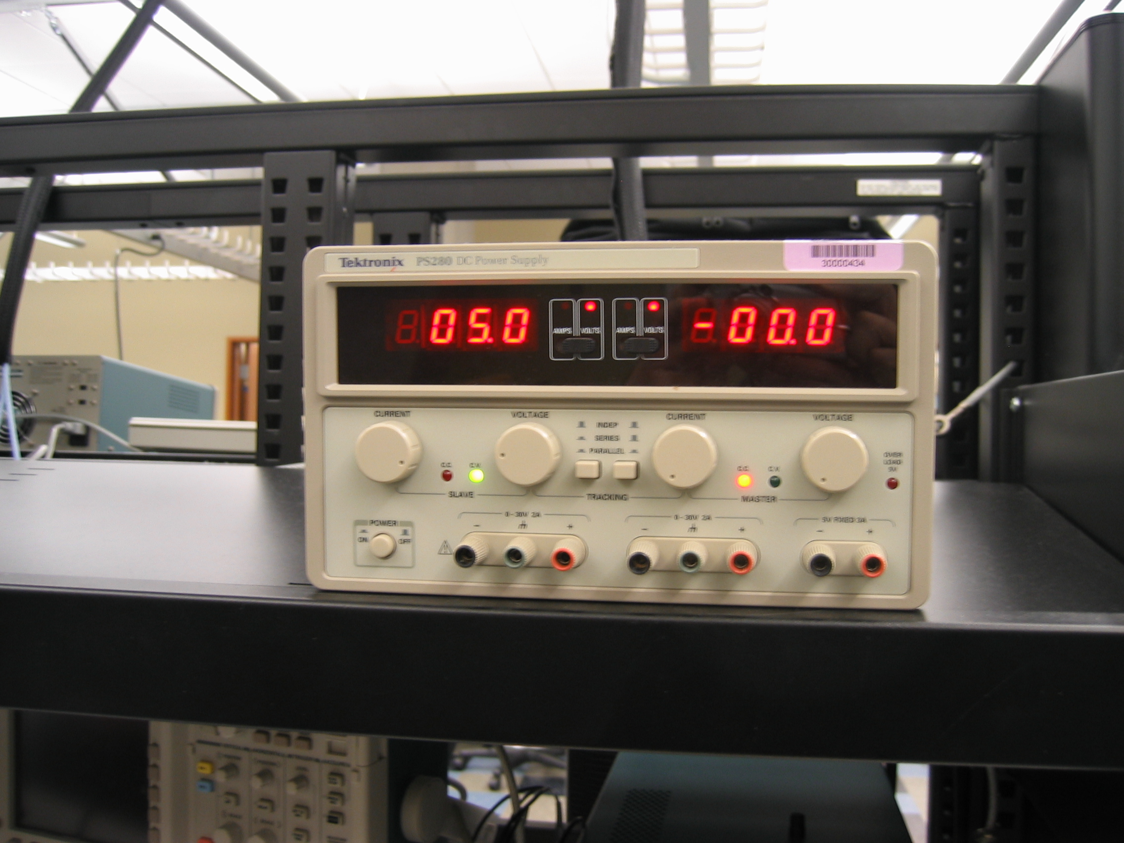
Turn off the power supply and connect it to the breadboard. The power supply has several connections on it. The one you want to use is the far left set (which is 3 plugs). The left plug is ground. Ignore the middle plug. The right plug is Vdd. Turn on the power supply.
Next, MAKE SURE THE FREQUENCY GENERATOR IS DISCONNECTED, and turn on the frequency generator. Press the "Func" button and set it to generate a square wave then press enter. Do the same with "Freq", "Ampl", and "Offset" to set amplitude to 2.5V, 1.25V offset, and 100K frequency. The screen should look like this:

Attach the cable to the ch1 output, and press the button marked ch1. The frequency generator cable has a positive and a negative output. Connect the negative output (black wire) to the ground connection of your board. Connect the positive output (red wire) to the input of your first inverter.(Use a wire as a connection point).
Turn on the oscilloscope. Each of the oscilloscope probes has a wire with an alligator clip that must be connected to ground. Connect channel 1 to the output of the frequency generator (i.e. the input of your first inverter). Connect channel 2 to the output of your first inverter. Make these connections with the probe clamps. It will look something like:

Tap "Autoset" on the oscilloscope. This will put the oscilloscope close to the right settings for you. It is not perfect, however. Thus be sure to set the vertical amplitude on both channels 1 and 2 to 5V and adjust the vertical offset and horizontal scale to your liking. You should see something like this.

At this point you should freely experiment with the power-supply, frequency
generator, and oscilloscope with the following limitations:
The above limitations will keep you from burning up the 4007 chip
Once you have satisfied yourself that you are generally comfortable with the equipment and setup your next step is to perform some measurements. Return the configuration back to the base one (5.0V amplitude / 2.5V offset / 100K frequency / 5V on the power supply).
When making the following graphs, you should sample 8 - 10 data points.
Set the frequency generator to use the triangle function. This will simulate a ramping input, and you will determine how this affects the output of the circuit that you have built.
Place the channel 1 probe on to the output of the frequency generator. Place the channel 2 probe on the output of the first inverter. Plot the input on the x-axis and the output on the y-axis of the same graph.
We will be measuring the response of our inverter to changes in voltage.
Switch the frequency generator function back to a square wave.
Place the channel 1 probe on to the output of the frequency generator. Place the channel 2 probe on the output of the second inverter. Starting with the power supply set to 5V (or 5.5v) measure the delay between the input of the circuit and the output. To do this accurately, use the ``cursor'' feature on the oscilloscope. Click the "Cursor" button near ``V bars''. Using the top knob move the cursors on the screen and measure difference in time of the falling edges. Record this value.
Slowly step the voltage by 1V at time up to 15V and record the delay at each voltage level.
Note: You may need to use the zoom feature of the oscilloscope (Magnifying glass button)
Using Excel (or paper), make a graph of your measured results. The x-axis of the graph should be supply voltage. The y-axis of the graph will be time.
What is the curve like?
Next turn the voltage back to 7V. Insert a 0.002uF capacitor between the output of the first inverter and ground. Make the same type of delay measurements at 1V increments between 7V and 15V. Once again make a graph of these measurements.
Was there ever a point where the inverter completely stopped working?
Return the system to its base configuration (2.5V amplitude / 1.25V offset / 100K frequency / 5V on the power supply). Connect the oscilloscope probe to the ground plane on the breadboard right next to pin 7 on the chip -- connect the ground on the probe as close to the power supply ground as possible. Increase the vertical resolution on the oscilloscope until you see the input clock noise appearing on the ground plane. What is the magnitude of this noise? Increase the frequency on the function generator up to 16M (its peak). Does the magnitude of the noise on the ground plane increase? Increase the amplitude on the frequency generator up to 5V (set the offset to 5V as well). What is the magnitude of the noise on the ground plane now?